- 您现在的位置:买卖IC网 > PDF目录18820 > MAX11008BETM+ (Maxim Integrated)IC CTLR LDMOS BIAS DUAL 48TQFN PDF资料下载
参数资料
| 型号: | MAX11008BETM+ |
| 厂商: | Maxim Integrated |
| 文件页数: | 8/67页 |
| 文件大小: | 0K |
| 描述: | IC CTLR LDMOS BIAS DUAL 48TQFN |
| 产品培训模块: | Lead (SnPb) Finish for COTS Obsolescence Mitigation Program |
| 标准包装: | 43 |
| 功能: | 偏压控制器 |
| RF 型: | 手机 |
| 次要属性: | 片上 4Kb EEPROM |
| 封装/外壳: | 48-WFQFN 裸露焊盘 |
| 包装: | 托盘 |
第1页第2页第3页第4页第5页第6页第7页当前第8页第9页第10页第11页第12页第13页第14页第15页第16页第17页第18页第19页第20页第21页第22页第23页第24页第25页第26页第27页第28页第29页第30页第31页第32页第33页第34页第35页第36页第37页第38页第39页第40页第41页第42页第43页第44页第45页第46页第47页第48页第49页第50页第51页第52页第53页第54页第55页第56页第57页第58页第59页第60页第61页第62页第63页第64页第65页第66页第67页
�� �
�
�Dual� RF� LDMOS� Bias� Controller� with�
�Nonvolatile� Memory�
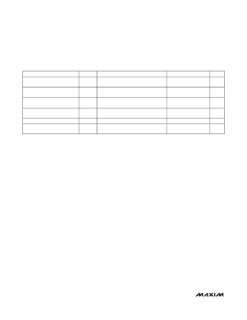
�MISCELLANEOUS� TIMING� CHARACTERISTICS� (Note� 15)� (continued)�
�(DV� DD� =� +2.7V� to� +5.25V,� AV� DD� =� +4.75V� to� +5.25V,� V� DGND� =� V� AGND� =� 0,� external� V� REFADC� =� +2.5V,� external� V� REFDAC� =� +2.5V,�
�C� REF� =� 0.1μF,� T� A� =� -40°C� to� +85°C,� unless� otherwise� noted.)�
�PARAMETER�
�SYMBOL�
�CONDITIONS�
�MIN�
�TYP�
�MAX�
�UNITS�
�DAC� Power-Up� Time� (External�
�Reference)�
�DAC� Power-Up� Time� (Internal�
�Reference)�
�Acquisition� Time� (Internally� Timed�
�in� ADC� Clock� Modes� 00� or� 01)�
�t� DPUEXT�
�t� DPUINT�
�t� ACQ�
�2�
�70�
�0.6�
�μs�
�μs�
�μs�
�Conversion� Time� (Internally�
�Clocked)�
�Delay� to� Start� of� Conversion� Time�
�Temperature� Conversion� Time�
�(Internally� Clocked)�
�t� CONV�
�t� CONVW�
�t� CONVT�
�Internally� clocked,� T� A� =� +25°C�
�(Note� 23)�
�1.3�
�70�
�10�
�μs�
�μs�
�μs�
�Note� 1:� Output� settles� to� within� ±0.5%� of� final� value.�
�Note� 2:� Total� unadjusted� errors� are� for� the� entire� gate-drive� channel� including� the� 12-bit� DAC,� and� the� gate� driver� is� measured� at�
�the� GATE1� and� GATE2� outputs.�
�Note� 3:� V� GATE_� =� V� DD� -� 0.1.� Measured� from� when� OPSAFE1� or� OPSAFE2� is� set� high.�
�Note� 4:� During� power-on-reset,� the� output� safe� switch� is� closed.� The� output� safe� switch� is� opened� under� user� software� control.�
�Note� 5:� Guaranteed� to� be� 11� bits� linearly� accurate.�
�Note� 6:� Offset� nulled.�
�Note� 7:� The� absolute� range� for� analog� inputs� is� from� 0� to� V� AVDD� .�
�Note� 8:� Internal� temperature-sensor� performance� is� guaranteed� by� design.�
�Note� 9:� The� MAX11008� and� the� external� sensor� are� at� the� same� ambient� temperature.� External� sensor� measurement� error� is� tested�
�with� a� diode-connected� 2N3904.�
�Note� 10:� Guaranteed� monotonicity.� Accuracy� is� degraded� at� lower� V� REFDAC� .�
�Note� 11:� SDA/DIN� is� an� open-drain� output� only� when� in� I� 2� C� mode.� A1/DOUT� is� an� open-drain� output� only� when� in� SPI� mode.�
�Note� 12:� Supply-current� limits� are� valid� only� when� digital� inputs� are� set� to� DGND� or� supply� voltage.� Timing� specifications� are� only�
�guaranteed� when� inputs� are� driven� rail-to-rail.�
�Note� 13:� Shutdown� supply� currents� are� typically� 0.4μA� for� AV� DD� ;� maximum� specification� is� limited� by� automated� test� equipment.�
�Note� 14:� All� times� are� referred� to� the� 50%� point� between� V� IH� and� V� IL� levels.�
�Note� 15:� Guaranteed� by� design.� Not� production� tested.�
�Note� 16:� DOUT� will� go� into� three-state� mode� after� the� CS� rising� edge.� Keep� CS� low� long� enough� for� the� DOUT� value� to� be� sampled�
�before� it� goes� to� three-state.�
�Note� 17:� A� master� device� must� provide� a� hold� time� of� at� least� 300ns� for� the� SDA� signal� (referred� to� V� IL� of� the� SCL� signal)� to� bridge�
�the� undefined� region� of� SCL’s� falling� edge.�
�Note� 18:� t� R� and� t� F� measured� between� 0.3� x� DV� DD� and� 0.7� x� DV� DD� .�
�Note� 19:� C� B� =� total� capacitance� of� one� bus� line� in� pF.� For� bus� loads� between� 100pF� and� 400pF,� the� timing� parameters� should� be�
�linearly� interpolated.�
�Note� 20:� An� appropriate� bus� pullup� resistance� must� be� selected� depending� on� board� capacitance.�
�Note� 21:� Input� filters� on� the� SDA� and� SCL� inputs� suppress� noise� spikes� less� than� 50ns.�
�Note� 22:� When� a� command� is� written� to� the� serial� interface,� the� command� is� passed� by� the� internal� oscillator� clock� and� executed.�
�There� is� a� small� synchronization� delay� before� the� new� value� is� written� to� the� appropriate� register.� If� the� serial� interface�
�attempts� to� read� the� new� value� back� before� t� RDBK� ,� the� new� data� is� not� corrupted;� however,� the� result� of� the� read� command�
�may� not� reflect� the� new� value.�
�Note� 23:� This� is� the� minimum� time� from� the� end� of� a� command� before� CNVST� should� be� asserted.� The� time� allows� for� the� data� from�
�the� preceding� write� to� arrive� and� set� up� the� chip� in� preparation� for� the� CNVST� .� The� time� need� only� be� observed� when� the�
�write� affects� the� ADC� controls.� Failure� to� observe� this� time� may� lead� to� incorrect� conversions� (for� example,� conversion� of�
�the� wrong� ADC� channel).�
�8�
�_______________________________________________________________________________________�
�相关PDF资料 |
PDF描述 |
|---|---|
| MCD310-16IO1 | MOD THYRISTOR/DIODE 1600V Y2-DCB |
| AH173-WL-7-B | IC HALL SENSOR LATCH 25MA SC59-3 |
| ACH3218-151-TD01 | FILTER 3-TERM 240MHZ 1.5A SMD |
| ND431425 | SCR MOD ISO DUAL 1400V 250A |
| AH175-WL-7-B | IC HALL SENSOR LATCH 25MA SC59-3 |
相关代理商/技术参数 |
参数描述 |
|---|---|
| MAX11008BETM+ | 功能描述:射频放大器 Dual RF LDMOS Bias Controller w/NV Mem RoHS:否 制造商:Skyworks Solutions, Inc. 类型:Low Noise Amplifier 工作频率:2.3 GHz to 2.8 GHz P1dB:18.5 dBm 输出截获点:37.5 dBm 功率增益类型:32 dB 噪声系数:0.85 dB 工作电源电压:5 V 电源电流:125 mA 测试频率:2.6 GHz 最大工作温度:+ 85 C 安装风格:SMD/SMT 封装 / 箱体:QFN-16 封装:Reel |
| MAX11008BETM+T | 功能描述:射频放大器 Dual RF LDMOS Bias Controller w/NV Mem RoHS:否 制造商:Skyworks Solutions, Inc. 类型:Low Noise Amplifier 工作频率:2.3 GHz to 2.8 GHz P1dB:18.5 dBm 输出截获点:37.5 dBm 功率增益类型:32 dB 噪声系数:0.85 dB 工作电源电压:5 V 电源电流:125 mA 测试频率:2.6 GHz 最大工作温度:+ 85 C 安装风格:SMD/SMT 封装 / 箱体:QFN-16 封装:Reel |
| MAX11008EVC16 | 功能描述:放大器 IC 开发工具 MAX11008 Eval Kit RoHS:否 制造商:International Rectifier 产品:Demonstration Boards 类型:Power Amplifiers 工具用于评估:IR4302 工作电源电压:13 V to 23 V |
| MAX11008EVKIT+ | 功能描述:放大器 IC 开发工具 MAX11008 Eval Kit RoHS:否 制造商:International Rectifier 产品:Demonstration Boards 类型:Power Amplifiers 工具用于评估:IR4302 工作电源电压:13 V to 23 V |
| MAX1100CWG | 制造商:Rochester Electronics LLC 功能描述: 制造商:Maxim Integrated Products 功能描述: |
发布紧急采购,3分钟左右您将得到回复。