- 您现在的位置:买卖IC网 > PDF目录5135 > MAX17482GTL+T (Maxim Integrated Products)IC CTLR PWM DUAL IMVP-6.5 40TQFN PDF资料下载
参数资料
| 型号: | MAX17482GTL+T |
| 厂商: | Maxim Integrated Products |
| 文件页数: | 41/48页 |
| 文件大小: | 0K |
| 描述: | IC CTLR PWM DUAL IMVP-6.5 40TQFN |
| 产品培训模块: | Lead (SnPb) Finish for COTS Obsolescence Mitigation Program |
| 标准包装: | 2,500 |
| 系列: | Quick-PWM™ |
| 应用: | 控制器,Intel IMVP-6,IMVP-6.5? |
| 输入电压: | 4.5 V ~ 5.5 V |
| 输出数: | 1 |
| 输出电压: | 0.013 V ~ 1.5 V |
| 工作温度: | -40°C ~ 105°C |
| 安装类型: | 表面贴装 |
| 封装/外壳: | 40-WFQFN 裸露焊盘 |
| 供应商设备封装: | 40-TQFN-EP(5x5) |
| 包装: | 带卷 (TR) |
第1页第2页第3页第4页第5页第6页第7页第8页第9页第10页第11页第12页第13页第14页第15页第16页第17页第18页第19页第20页第21页第22页第23页第24页第25页第26页第27页第28页第29页第30页第31页第32页第33页第34页第35页第36页第37页第38页第39页第40页当前第41页第42页第43页第44页第45页第46页第47页第48页
�� �
�
�Dual-Phase,� Quick-PWM� Controllers� for�
�IMVP-6+/IMVP-6.5� CPU� Core� Power� Supplies�
�?�
�Input-voltage� range:� The� maximum� value�
�(V� IN(MAX)� )� must� accommodate� the� worst-case� high�
�AC� adapter� voltage.� The� minimum� value� (V� IN(MIN)� )�
�must� account� for� the� lowest� input� voltage� after� drops�
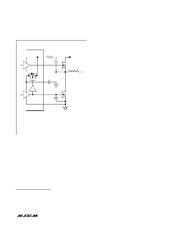
�BST_�
�(R� BST_� )*�
�INPUT� (V� IN� )�
�due� to� connectors,� fuses,� and� battery� selector�
�switches.� If� there� is� a� choice� at� all,� lower� input� volt-�
�DH_�
�LX_�
�C� BST_�
�N� H�
�L�
�?�
�ages� result� in� better� efficiency.�
�Maximum� load� current:� There� are� two� values� to�
�consider.� The� peak� load� current� (I� LOAD(MAX)� )� deter-�
�mines� the� instantaneous� component� stresses� and� fil-�
�tering� requirements,� and� thus� drives� output�
�V� DD�
�C� BYP�
�capacitor� selection,� inductor� saturation� rating,� and�
�the� design� of� the� current-limit� circuit.� The� continuous�
�load� current� (I� LOAD� )� determines� the� thermal� stress-�
�es� and� thus� drives� the� selection� of� input� capacitors,�
�MOSFETs,� and� other� critical� heat-contributing� com-�
�DL_�
�N� L�
�ponents.� Modern� notebook� CPUs� generally� exhibit�
�PGND�
�(C� NL� )*�
�?�
�I� LOAD� =� I� LOAD(MAX)� x� 80%.�
�For� multiphase� systems,� each� phase� supports� a�
�fraction� of� the� load,� depending� on� the� current� bal-�
�ancing.� When� properly� balanced,� the� load� current� is�
�evenly� distributed� among� each� phase:�
�I� LOAD� (� PHASE� )� =� LOAD�
�(R� BST_� )* OPTIONAL—THE RESISTOR LOWERS EMI BY DECREASING THE�
�SWITCHING� NODE� RISE� TIME.�
�(C� NL� )*� OPTIONAL—THE� CAPACITOR� REDUCES� LX_� TO� DL_� CAPACITIVE�
�COUPLING� THAT� CAN� CAUSE� SHOOT-THROUGH� CURRENTS.�
�Figure� 11.� Gate� Drive� Circuit�
�?�
�I�
�η� TOTAL�
�where� η� TOTAL� is� the� total� number� of� active� phases.�
�Switching� frequency:� This� choice� determines� the�
�basic� trade-off� between� size� and� efficiency.� The�
�optimal� frequency� is� largely� a� function� of� maximum�
�Alternatively,� shoot-through� currents� can� be� caused� by�
�a� combination� of� fast� high-side� MOSFETs� and� slow� low-�
�side� MOSFETs.� If� the� turn-off� delay� time� of� the� low-side�
�MOSFETs� are� too� long,� the� high-side� MOSFETs� can�
�turn� on� before� the� low-side� MOSFETs� have� actually�
�turned� off.� Adding� a� resistor� less� than� 5� Ω� in� series� with�
�BST_� slows� down� the� high-side� MOSFET� turn-on� time,�
�eliminating� the� shoot-through� currents� without� degrad-�
�ing� the� turn-off� time� (R� BST_� in� Figure� 11).� Slowing� down�
�the� high-side� MOSFET� also� reduces� the� LX_� node� rise�
�time,� thereby� reducing� EMI� and� high-frequency� cou-�
�pling� responsible� for� switching� noise.�
�Multiphase� Quick-PWM�
�Design� Procedure�
�Firmly� establish� the� input-voltage� range� and� maximum�
�load� current� before� choosing� a� switching� frequency�
�and� inductor� operating� point� (ripple-current� ratio).� The�
�primary� design� trade-off� lies� in� choosing� a� good� switch-�
�ing� frequency� and� inductor� operating� point,� and� the� fol-�
�lowing� four� factors� dictate� the� rest� of� the� design:�
�?�
�input� voltage,� due� to� MOSFET� switching� losses� that�
�are� proportional� to� frequency� and� V� IN� 2� .� The� opti-�
�mum� frequency� is� also� a� moving� target� due� to� rapid�
�improvements� in� MOSFET� technology� that� are� mak-�
�ing� higher� frequencies� more� practical.�
�Inductor� operating� point:� This� choice� provides�
�trade-offs� between� size� vs.� efficiency� and� transient�
�response� vs.� output� noise.� Low� inductor� values� pro-�
�vide� better� transient� response� and� smaller� physical�
�size,� but� also� result� in� lower� efficiency� and� higher�
�output� noise� due� to� increased� ripple� current.� The�
�minimum� practical� inductor� value� is� one� that� causes�
�the� circuit� to� operate� at� the� edge� of� critical� conduc-�
�tion� (where� the� inductor� current� just� touches� zero�
�with� every� cycle� at� maximum� load).� Inductor� values�
�lower� than� this� grant� no� further� size-reduction� bene-�
�fit.� The� optimum� operating� point� is� usually� found�
�between� 20%� and� 50%� ripple� current.�
�______________________________________________________________________________________�
�41�
�相关PDF资料 |
PDF描述 |
|---|---|
| 200MXG2200MEFCSN35X45 | CAP ALUM 2200UF 200V 20% SNAP-IN |
| MAX17082GTL+T | IC CTLR PWM DUAL IMVP-6.5 40TQFN |
| HMC13DRAS | CONN EDGECARD 26POS R/A .100 SLD |
| 250VXH1800MEFCSN35X50 | CAP ALUM 1800UF 250V 20% SNAP-IN |
| 250MXG1800MEFCSN35X50 | CAP ALUM 1800UF 250V 20% SNAP-IN |
相关代理商/技术参数 |
参数描述 |
|---|---|
| MAX1748EUE | 功能描述:直流/直流开关转换器 RoHS:否 制造商:STMicroelectronics 最大输入电压:4.5 V 开关频率:1.5 MHz 输出电压:4.6 V 输出电流:250 mA 输出端数量:2 最大工作温度:+ 85 C 安装风格:SMD/SMT |
| MAX1748EUE+ | 功能描述:直流/直流开关转换器 Triple-Output TFT LCD DC/DC Converters RoHS:否 制造商:STMicroelectronics 最大输入电压:4.5 V 开关频率:1.5 MHz 输出电压:4.6 V 输出电流:250 mA 输出端数量:2 最大工作温度:+ 85 C 安装风格:SMD/SMT |
| MAX1748EUE+T | 功能描述:直流/直流开关转换器 Triple-Output TFT LCD DC/DC Converters RoHS:否 制造商:STMicroelectronics 最大输入电压:4.5 V 开关频率:1.5 MHz 输出电压:4.6 V 输出电流:250 mA 输出端数量:2 最大工作温度:+ 85 C 安装风格:SMD/SMT |
| MAX1748EUE-T | 功能描述:直流/直流开关转换器 RoHS:否 制造商:STMicroelectronics 最大输入电压:4.5 V 开关频率:1.5 MHz 输出电压:4.6 V 输出电流:250 mA 输出端数量:2 最大工作温度:+ 85 C 安装风格:SMD/SMT |
| MAX1748EUE-TG069 | 制造商:Rochester Electronics LLC 功能描述: 制造商:Maxim Integrated Products 功能描述: |
发布紧急采购,3分钟左右您将得到回复。