- 您现在的位置:买卖IC网 > PDF目录80585 > MB9AF312NPMC 32-BIT, FLASH, 40 MHz, RISC MICROCONTROLLER, PQFP100 PDF资料下载
参数资料
| 型号: | MB9AF312NPMC |
| 元件分类: | 微控制器/微处理器 |
| 英文描述: | 32-BIT, FLASH, 40 MHz, RISC MICROCONTROLLER, PQFP100 |
| 封装: | 0.50 MM PITCH, PLASTIC, LQFP-100 |
| 文件页数: | 78/114页 |
| 文件大小: | 1357K |
| 代理商: | MB9AF312NPMC |
第1页第2页第3页第4页第5页第6页第7页第8页第9页第10页第11页第12页第13页第14页第15页第16页第17页第18页第19页第20页第21页第22页第23页第24页第25页第26页第27页第28页第29页第30页第31页第32页第33页第34页第35页第36页第37页第38页第39页第40页第41页第42页第43页第44页第45页第46页第47页第48页第49页第50页第51页第52页第53页第54页第55页第56页第57页第58页第59页第60页第61页第62页第63页第64页第65页第66页第67页第68页第69页第70页第71页第72页第73页第74页第75页第76页第77页当前第78页第79页第80页第81页第82页第83页第84页第85页第86页第87页第88页第89页第90页第91页第92页第93页第94页第95页第96页第97页第98页第99页第100页第101页第102页第103页第104页第105页第106页第107页第108页第109页第110页第111页第112页第113页第114页
ATmega48PA/88PA/168PA [DATASHEET]
9223F–AVR–04/14
66
14.2.2 Toggling the Pin
Writing a logic one to PINxn toggles the value of PORTxn, independent on the value of DDRxn. Note that the SBI instruction
can be used to toggle one single bit in a port.
14.2.3 Switching Between Input and Output
When switching between tri-state ({DDxn, PORTxn} = 0b00) and output high ({DDxn, PORTxn} = 0b11), an intermediate
state with either pull-up enabled {DDxn, PORTxn} = 0b01) or output low ({DDxn, PORTxn} = 0b10) must occur. Normally, the
pull-up enabled state is fully acceptable, as a high-impedance environment will not notice the difference between a strong
high driver and a pull-up. If this is not the case, the PUD bit in the MCUCR register can be set to disable all pull-ups in all
ports.
Switching between input with pull-up and output low generates the same problem. The user must use either the tri-state
({DDxn, PORTxn} = 0b00) or the output high state ({DDxn, PORTxn} = 0b11) as an intermediate step.
Table 14-1 summarizes the control signals for the pin value.
14.2.4 Reading the Pin Value
Independent of the setting of data direction bit DDxn, the port pin can be read through the PINxn register bit. As shown in
Figure 14-2 on page 65, the PINxn register bit and the preceding latch constitute a synchronizer. This is needed to avoid
metastability if the physical pin changes value near the edge of the internal clock, but it also introduces a delay. Figure 14-3
shows a timing diagram of the synchronization when reading an externally applied pin value. The maximum and minimum
propagation delays are denoted tpd,max and tpd,min respectively.
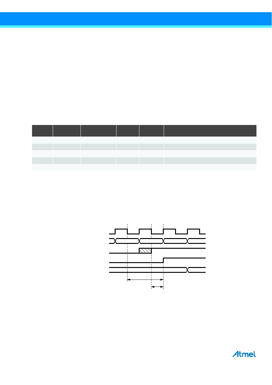
Figure 14-3. Synchronization when Reading an Externally Applied Pin value
Consider the clock period starting shortly after the first falling edge of the system clock. The latch is closed when the clock is
low, and goes transparent when the clock is high, as indicated by the shaded region of the “SYNC LATCH” signal. The signal
value is latched when the system clock goes low. It is clocked into the PINxn register at the succeeding positive clock edge.
As indicated by the two arrows tpd,max and tpd,min, a single signal transition on the pin will be delayed between and 1
system clock period depending upon the time of assertion.
Table 14-1. Port Pin Configurations
DDxn
PORTxn
PUD
(in MCUCR)
I/O
Pull-up
Comment
0
X
Input
No
Tri-state (Hi-Z)
0
1
0
Input
Yes
Pxn will source current if ext. pulled low.
0
1
Input
No
Tri-state (Hi-Z)
1
0
X
Output
No
Output low (sink)
1
X
Output
No
Output high (source)
SYSTEM CLK
INSTRUCTIONS
SYNC LATCH
PINxn
r17
XXX
0x00
0xFF
in r17, PINx
t
pd, max
t
pd, min
相关PDF资料 |
PDF描述 |
|---|---|
| MB9AF315NPF | 32-BIT, FLASH, 40 MHz, RISC MICROCONTROLLER, PQFP100 |
| MSM65P514-JS | 8-BIT, OTPROM, 12 MHz, MICROCONTROLLER, PQCC68 |
| MSM67P620-JS | 16-BIT, OTPROM, 10 MHz, MICROCONTROLLER, PQCC68 |
| MSM80C154-RS | 8-BIT, 12 MHz, MICROCONTROLLER, PDIP40 |
| MSM83C154-RS | 8-BIT, MROM, 12 MHz, MICROCONTROLLER, PDIP40 |
相关代理商/技术参数 |
参数描述 |
|---|---|
| MB9AF314LAPMC1-G-JNE2 | 制造商:FUJITSU 功能描述: |
| MB9AF314LAPMC-G-JNE2 | 制造商:Fujitsu 功能描述:Bulk |
| MB9AF314LAQN-G-AVE2 | 功能描述:ARM? Cortex?-M3 FM3 MB9A310A Microcontroller IC 32-Bit 40MHz 256KB (256K x 8) FLASH 64-QFN Exposed Pad (9x9) 制造商:cypress semiconductor corp 系列:FM3 MB9A310A 包装:托盘 零件状态:有效 核心处理器:ARM? Cortex?-M3 核心尺寸:32-位 速度:40MHz 连接性:CSIO,I2C,LIN,UART/USART,USB 外设:DMA,LVD,POR,PWM,WDT I/O 数:51 程序存储容量:256KB(256K x 8) 程序存储器类型:闪存 EEPROM 容量:- RAM 容量:32K x 8 电压 - 电源(Vcc/Vdd):2.7 V ~ 5.5 V 数据转换器:A/D 9x12b 振荡器类型:内部 工作温度:-40°C ~ 105°C(TA) 封装/外壳:64-VFQFN 裸露焊盘 供应商器件封装:64-QFN 裸露焊盘(9x9) 标准包装:260 |
| MB9AF314LPMC1-ESE1 | 制造商:FUJITSU 功能描述: |
| MB9AF314LPMC1-GE1 | 制造商:FUJITSU 功能描述: |
发布紧急采购,3分钟左右您将得到回复。