- 您现在的位置:买卖IC网 > PDF目录80366 > MB9AF314NBGL 32-BIT, FLASH, 40 MHz, RISC MICROCONTROLLER, PBGA112 PDF资料下载
参数资料
| 型号: | MB9AF314NBGL |
| 元件分类: | 微控制器/微处理器 |
| 英文描述: | 32-BIT, FLASH, 40 MHz, RISC MICROCONTROLLER, PBGA112 |
| 封装: | 0.80 MM PITCH, PLASTIC, FBGA-112 |
| 文件页数: | 18/114页 |
| 文件大小: | 1357K |
| 代理商: | MB9AF314NBGL |
第1页第2页第3页第4页第5页第6页第7页第8页第9页第10页第11页第12页第13页第14页第15页第16页第17页当前第18页第19页第20页第21页第22页第23页第24页第25页第26页第27页第28页第29页第30页第31页第32页第33页第34页第35页第36页第37页第38页第39页第40页第41页第42页第43页第44页第45页第46页第47页第48页第49页第50页第51页第52页第53页第54页第55页第56页第57页第58页第59页第60页第61页第62页第63页第64页第65页第66页第67页第68页第69页第70页第71页第72页第73页第74页第75页第76页第77页第78页第79页第80页第81页第82页第83页第84页第85页第86页第87页第88页第89页第90页第91页第92页第93页第94页第95页第96页第97页第98页第99页第100页第101页第102页第103页第104页第105页第106页第107页第108页第109页第110页第111页第112页第113页第114页
ATmega48PA/88PA/168PA [DATASHEET]
9223F–AVR–04/14
114
The Timer/Counter overflow flag (TOV1) is set at the same timer clock cycle as the OCR1x registers are updated with the
double buffer value (at BOTTOM). When either OCR1A or ICR1 is used for defining the TOP value, the OC1A or ICF1 flag
set when TCNT1 has reached TOP. The interrupt flags can then be used to generate an interrupt each time the counter
reaches the TOP or BOTTOM value.
When changing the TOP value the program must ensure that the new TOP value is higher or equal to the value of all of the
compare registers. If the TOP value is lower than any of the compare registers, a compare match will never occur between
the TCNT1 and the OCR1x.
As Figure 16-9 shows the output generated is, in contrast to the phase correct mode, symmetrical in all periods. Since the
OCR1x registers are updated at BOTTOM, the length of the rising and the falling slopes will always be equal. This gives
symmetrical output pulses and is therefore frequency correct.
Using the ICR1 register for defining TOP works well when using fixed TOP values. By using ICR1, the OCR1A register is
free to be used for generating a PWM output on OC1A. However, if the base PWM frequency is actively changed by
changing the TOP value, using the OCR1A as TOP is clearly a better choice due to its double buffer feature.
In phase and frequency correct PWM mode, the compare units allow generation of PWM waveforms on the OC1x pins.
Setting the COM1x1:0 bits to two will produce a non-inverted PWM and an inverted PWM output can be generated by setting
the COM1x1:0 to three (See Table on page 117). The actual OC1x value will only be visible on the port pin if the data
direction for the port pin is set as output (DDR_OC1x). The PWM waveform is generated by setting (or clearing) the OC1x
register at the compare match between OCR1x and TCNT1 when the counter increments, and clearing (or setting) the OC1x
register at compare match between OCR1x and TCNT1 when the counter decrements. The PWM frequency for the output
when using phase and frequency correct PWM can be calculated by the following equation:
The N variable represents the prescaler divider (1, 8, 64, 256, or 1024).
The extreme values for the OCR1x register represents special cases when generating a PWM waveform output in the phase
correct PWM mode. If the OCR1x is set equal to BOTTOM the output will be continuously low and if set equal to TOP the
output will be set to high for non-inverted PWM mode. For inverted PWM the output will have the opposite logic values. If
OCR1A is used to define the TOP value (WGM13:0 = 9) and COM1A1:0 = 1, the OC1A output will toggle with a 50% duty
cycle.
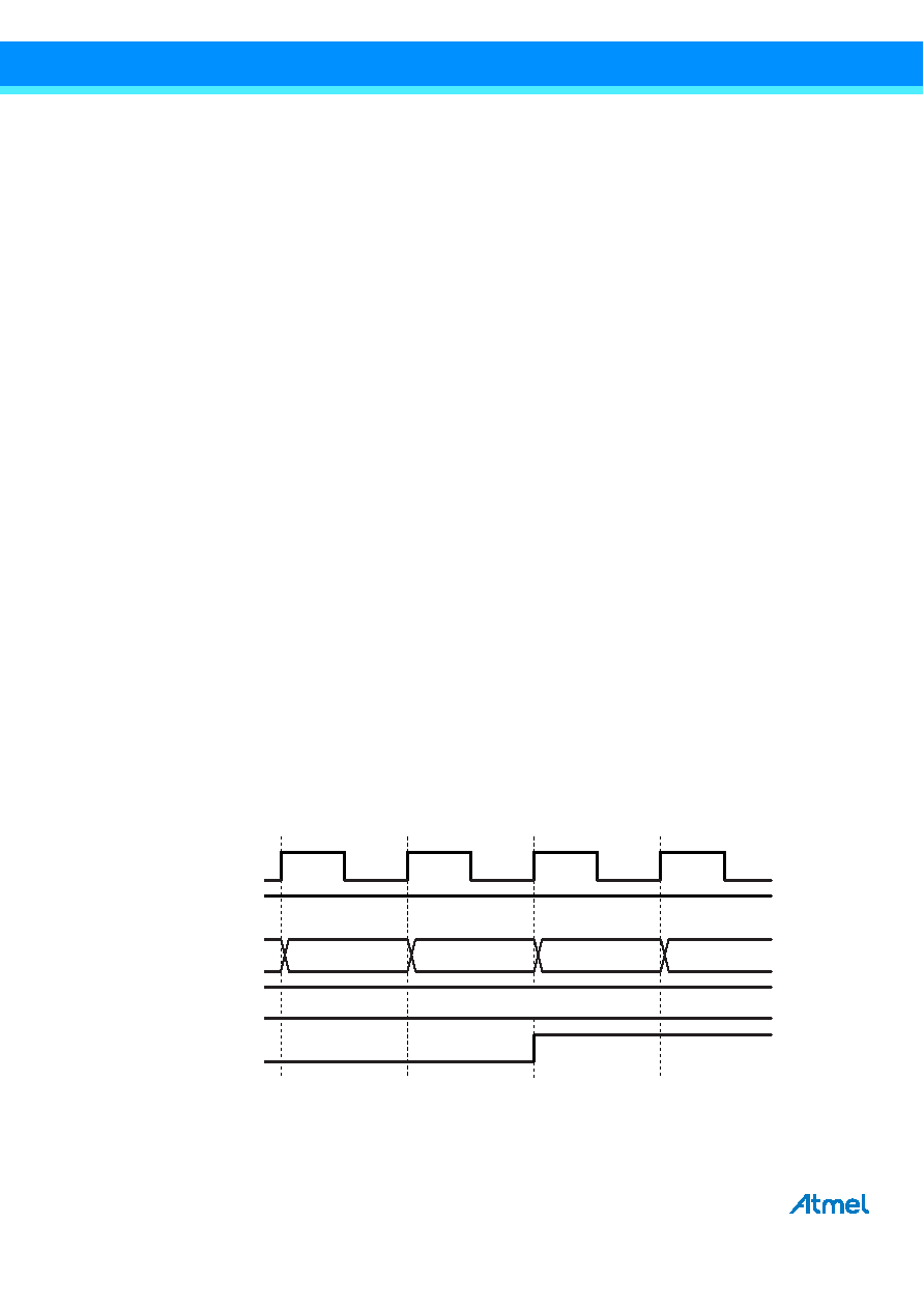
16.10 Timer/Counter Timing Diagrams
The Timer/Counter is a synchronous design and the timer clock (clkT1) is therefore shown as a clock enable signal in the
following figures. The figures include information on when interrupt flags are set, and when the OCR1x register is updated
with the OCR1x buffer value (only for modes utilizing double buffering). Figure 16-10 shows a timing diagram for the setting
of OCF1x.
Figure 16-10.Timer/Counter Timing Diagram, Setting of OCF1x, no Prescaling
fOCnxPFCPWM
fclk_I/O
2N
×
TOP
×
-------------------------------
=
OCRnx - 1
clkI/O
(clkI/O/1)
TCNTn
OCRnx
OCFnx
clkTn
OCRnx
OCRnx Value
OCRnx + 1
OCRnx + 2
相关PDF资料 |
PDF描述 |
|---|---|
| MB9BF418SPMC | RISC MICROCONTROLLER, PQFP144 |
| M38802M1-XXXFS | 8-BIT, MROM, 8 MHz, MICROCONTROLLER, CQCC64 |
| MAQ281CE | 16-BIT, MICROPROCESSOR, DMA64 |
| MAS281CS | 16-BIT, MICROPROCESSOR, DMA64 |
| M37730S2ASP | 16-BIT, 16 MHz, MICROCONTROLLER, PDIP64 |
相关代理商/技术参数 |
参数描述 |
|---|---|
| MB9AF314NBGL-GE1 | 制造商:FUJITSU 功能描述: 制造商:FUJITSU 功能描述:MCU 32BIT CORTEX-M3 FM3 112BGA 制造商:FUJITSU 功能描述:MCU, 32BIT, CORTEX-M3, FM3, 112BGA 制造商:FUJITSU 功能描述:MCU, 32BIT, CORTEX-M3, FM3, 112BGA, Controller Family/Series:ARM Cortex-M3, Core 制造商:FUJITSU 功能描述:MCU, 32BIT, CORTEX-M3, FM3, 112BGA, Controller Family/Series:ARM Cortex-M3, Core Size:32bit, No. of I/O's:83, Supply Voltage Min:2.7V, Supply Voltage Max:5.5V, Digital IC Case Style:BGA, No. of Pins:112, Program Memory Size:256KB, , RoHS Compliant: Yes |
| MB9AF314NPMC-GE1 | 制造商:FUJITSU 功能描述: |
| MB9AF314NPMC-G-JNE1 | 制造商:FUJITSU 功能描述: 制造商:FUJITSU 功能描述:MCU 32BIT CORTEX-M3 FM3 100LQFP 制造商:FUJITSU 功能描述:MCU, 32BIT, CORTEX-M3, FM3, 100LQFP, Controller Family/Series:ARM Cortex-M3, Cor |
| MB9AF316MAPMC-G-JNE2 | 制造商:Fujitsu 功能描述:Bulk |
| MB9AF316MPMC-G-JNE1 | 制造商:FUJITSU 功能描述:MCU 32BIT CORTEX-M3 FM3 80LQFP 制造商:FUJITSU 功能描述:MCU, 32BIT, CORTEX-M3, FM3, 80LQFP, Controller Family/Series:ARM Cortex-M3, Core |
发布紧急采购,3分钟左右您将得到回复。