- 您现在的位置:买卖IC网 > PDF目录80366 > MB9AF314NBGL 32-BIT, FLASH, 40 MHz, RISC MICROCONTROLLER, PBGA112 PDF资料下载
参数资料
| 型号: | MB9AF314NBGL |
| 元件分类: | 微控制器/微处理器 |
| 英文描述: | 32-BIT, FLASH, 40 MHz, RISC MICROCONTROLLER, PBGA112 |
| 封装: | 0.80 MM PITCH, PLASTIC, FBGA-112 |
| 文件页数: | 42/114页 |
| 文件大小: | 1357K |
| 代理商: | MB9AF314NBGL |
第1页第2页第3页第4页第5页第6页第7页第8页第9页第10页第11页第12页第13页第14页第15页第16页第17页第18页第19页第20页第21页第22页第23页第24页第25页第26页第27页第28页第29页第30页第31页第32页第33页第34页第35页第36页第37页第38页第39页第40页第41页当前第42页第43页第44页第45页第46页第47页第48页第49页第50页第51页第52页第53页第54页第55页第56页第57页第58页第59页第60页第61页第62页第63页第64页第65页第66页第67页第68页第69页第70页第71页第72页第73页第74页第75页第76页第77页第78页第79页第80页第81页第82页第83页第84页第85页第86页第87页第88页第89页第90页第91页第92页第93页第94页第95页第96页第97页第98页第99页第100页第101页第102页第103页第104页第105页第106页第107页第108页第109页第110页第111页第112页第113页第114页
33
ATmega48PA/88PA/168PA [DATASHEET]
9223F–AVR–04/14
9.12
Register Description
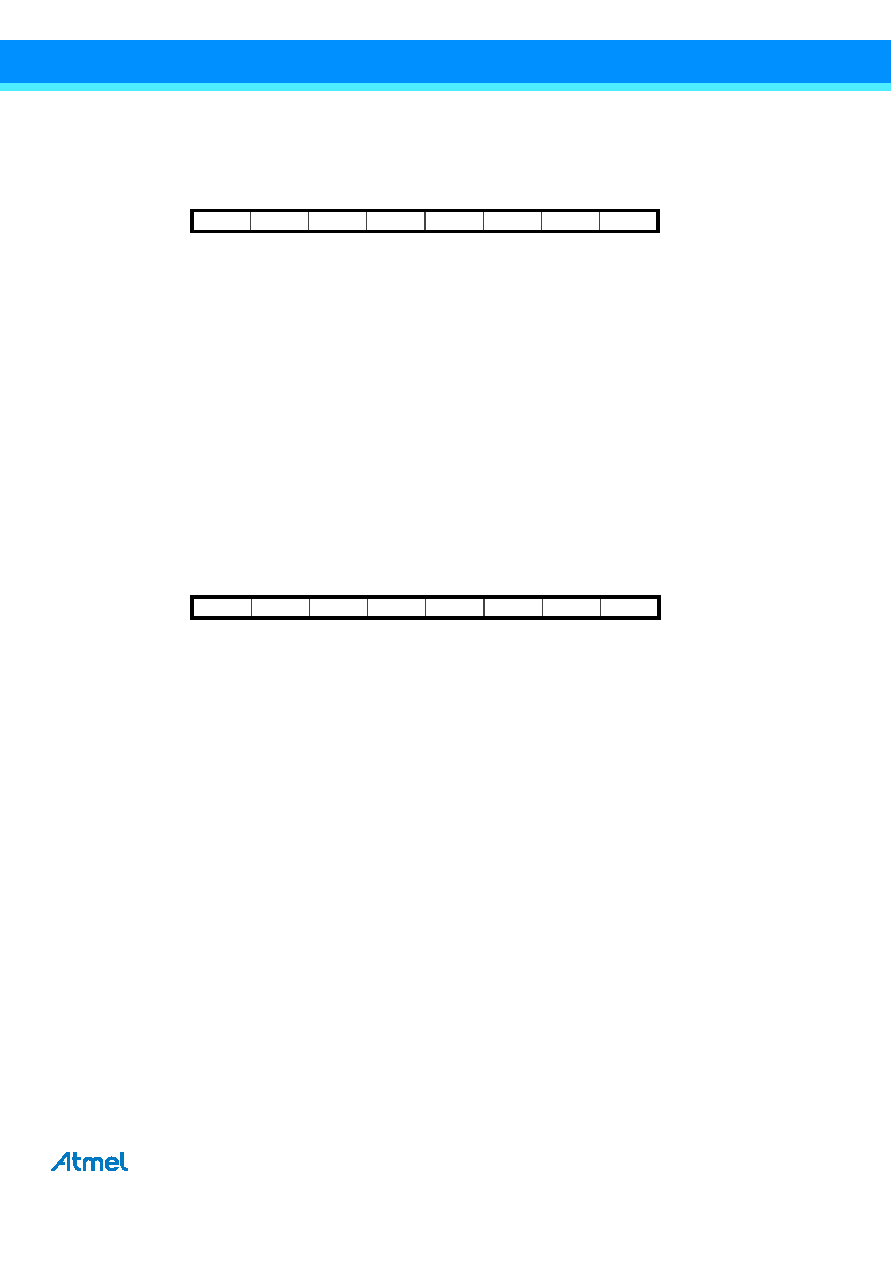
9.12.1 OSCCAL – Oscillator Calibration Register
Bits 7:0 – CAL[7:0]: Oscillator Calibration Value
The oscillator calibration register is used to trim the calibrated internal RC oscillator to remove process variations from the
oscillator frequency. A pre-programmed calibration value is automatically written to this register during chip reset, giving the
factory calibrated frequency as specified in Table 29-3 on page 271. The application software can write this register to
change the oscillator frequency. The oscillator can be calibrated to frequencies as specified in Table 29-3 on page 271.
Calibration outside that range is not guaranteed.
Note that this oscillator is used to time EEPROM and flash write accesses, and these write times will be affected accordingly.
If the EEPROM or flash are written, do not calibrate to more than 8.8MHz. Otherwise, the EEPROM or flash write may fail.
The CAL7 bit determines the range of operation for the oscillator. Setting this bit to 0 gives the lowest frequency range,
setting this bit to 1 gives the highest frequency range. The two frequency ranges are overlapping, in other words a setting of
OSCCAL = 0x7F gives a higher frequency than OSCCAL = 0x80.
The CAL6...0 bits are used to tune the frequency within the selected range. A setting of 0x00 gives the lowest frequency in
that range, and a setting of 0x7F gives the highest frequency in the range.
9.12.2 CLKPR – Clock Prescale Register
Bit 7 – CLKPCE: Clock Prescaler Change Enable
The CLKPCE bit must be written to logic one to enable change of the CLKPS bits. The CLKPCE bit is only updated when the
other bits in CLKPR are simultaneously written to zero. CLKPCE is cleared by hardware four cycles after it is written or when
CLKPS bits are written. Rewriting the CLKPCE bit within this time-out period does neither extend the time-out period, nor
clear the CLKPCE bit.
Bits 3:0 – CLKPS[3:0]: Clock Prescaler Select Bits 3 - 0
These bits define the division factor between the selected clock source and the internal system clock. These bits can be
written run-time to vary the clock frequency to suit the application requirements. As the divider divides the master clock input
to the MCU, the speed of all synchronous peripherals is reduced when a division factor is used. The division factors are
given in Table 9-17 on page 34.
Bit
7654
3210
CAL7
CAL6
CAL5
CAL4
CAL3
CAL2
CAL1
CAL0
OSCCAL
Read/Write
R/W
Initial Value
Device Specific Calibration Value
Bit
7
6543
2
1
0
CLKPCE
–
CLKPS3 CLKPS2 CLKPS1 CLKPS0
CLKPR
Read/Write
R/W
R
R/W
Initial Value
0
See Bit Description
相关PDF资料 |
PDF描述 |
|---|---|
| MB9BF418SPMC | RISC MICROCONTROLLER, PQFP144 |
| M38802M1-XXXFS | 8-BIT, MROM, 8 MHz, MICROCONTROLLER, CQCC64 |
| MAQ281CE | 16-BIT, MICROPROCESSOR, DMA64 |
| MAS281CS | 16-BIT, MICROPROCESSOR, DMA64 |
| M37730S2ASP | 16-BIT, 16 MHz, MICROCONTROLLER, PDIP64 |
相关代理商/技术参数 |
参数描述 |
|---|---|
| MB9AF314NBGL-GE1 | 制造商:FUJITSU 功能描述: 制造商:FUJITSU 功能描述:MCU 32BIT CORTEX-M3 FM3 112BGA 制造商:FUJITSU 功能描述:MCU, 32BIT, CORTEX-M3, FM3, 112BGA 制造商:FUJITSU 功能描述:MCU, 32BIT, CORTEX-M3, FM3, 112BGA, Controller Family/Series:ARM Cortex-M3, Core 制造商:FUJITSU 功能描述:MCU, 32BIT, CORTEX-M3, FM3, 112BGA, Controller Family/Series:ARM Cortex-M3, Core Size:32bit, No. of I/O's:83, Supply Voltage Min:2.7V, Supply Voltage Max:5.5V, Digital IC Case Style:BGA, No. of Pins:112, Program Memory Size:256KB, , RoHS Compliant: Yes |
| MB9AF314NPMC-GE1 | 制造商:FUJITSU 功能描述: |
| MB9AF314NPMC-G-JNE1 | 制造商:FUJITSU 功能描述: 制造商:FUJITSU 功能描述:MCU 32BIT CORTEX-M3 FM3 100LQFP 制造商:FUJITSU 功能描述:MCU, 32BIT, CORTEX-M3, FM3, 100LQFP, Controller Family/Series:ARM Cortex-M3, Cor |
| MB9AF316MAPMC-G-JNE2 | 制造商:Fujitsu 功能描述:Bulk |
| MB9AF316MPMC-G-JNE1 | 制造商:FUJITSU 功能描述:MCU 32BIT CORTEX-M3 FM3 80LQFP 制造商:FUJITSU 功能描述:MCU, 32BIT, CORTEX-M3, FM3, 80LQFP, Controller Family/Series:ARM Cortex-M3, Core |
发布紧急采购,3分钟左右您将得到回复。