- 您现在的位置:买卖IC网 > PDF目录16634 > MC33910G5AC (Freescale Semiconductor)IC SYSTEM BASIS CHIP 32LQFP PDF资料下载
参数资料
| 型号: | MC33910G5AC |
| 厂商: | Freescale Semiconductor |
| 文件页数: | 14/90页 |
| 文件大小: | 0K |
| 描述: | IC SYSTEM BASIS CHIP 32LQFP |
| 标准包装: | 250 |
| 应用: | 系统基础芯片 |
| 电流 - 电源: | 4.5mA |
| 电源电压: | 5.5 V ~ 27 V |
| 工作温度: | -40°C ~ 125°C |
| 安装类型: | 表面贴装 |
| 封装/外壳: | 32-LQFP |
| 供应商设备封装: | 32-LQFP(7x7) |
| 包装: | 托盘 |
第1页第2页第3页第4页第5页第6页第7页第8页第9页第10页第11页第12页第13页当前第14页第15页第16页第17页第18页第19页第20页第21页第22页第23页第24页第25页第26页第27页第28页第29页第30页第31页第32页第33页第34页第35页第36页第37页第38页第39页第40页第41页第42页第43页第44页第45页第46页第47页第48页第49页第50页第51页第52页第53页第54页第55页第56页第57页第58页第59页第60页第61页第62页第63页第64页第65页第66页第67页第68页第69页第70页第71页第72页第73页第74页第75页第76页第77页第78页第79页第80页第81页第82页第83页第84页第85页第86页第87页第88页第89页第90页
�� �
�
�MC33910G5AC/MC3433910G5AC�
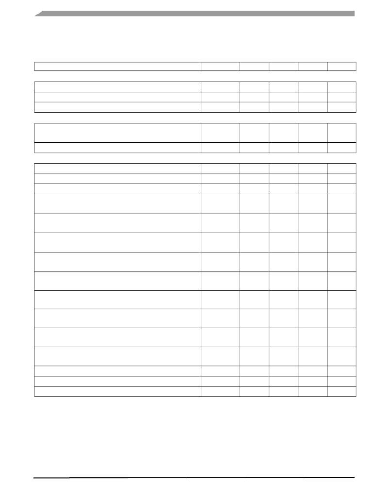
�ELECTRICAL� CHARACTERISTICS�
�STATIC� ELECTRICAL� CHARACTERISTICS�
�Table� 4.� Static� Electrical� Characteristics� (continued)�
�Characteristics� noted� under� conditions� 5.5� V� ≤� V� SUP� ≤� 18� V,� -40°C� ≤� T� A� ≤� 125°C� for� the� 33910� and� -40°C� ≤� T� A� ≤� 85°C� for� the�
�34910,� unless� otherwise� noted.� Typical� values� noted� reflect� the� approximate� parameter� mean� at� T� A� =� 25°C� under� nominal�
�conditions,� unless� otherwise� noted.�
�Characteristic�
�Symbol�
�Min�
�Typ�
�Max�
�Unit�
�TXD� INPUT� PIN� (LIN� PHYSICAL� LAYER)� (TXD)�
�Low-state� Input� Voltage�
�High-state� Input� Voltage�
�Pin� Pull-up� Current,� 0� V� <� V� IN� <� 3.5� V�
�V� IL�
�V� IH�
�I� PUIN�
�-0.3�
�0.7� x� V� DD�
�10�
�–�
�–�
�20�
�0.3� x� V� DD�
�V� DD� +0.3�
�30�
�V�
�V�
�μA�
�LIN� PHYSICAL� LAYER� WITH� J2602� FEATURE� ENABLED� (BIT� DIS_J2602� =� 0)�
�LIN� Under� Voltage� threshold�
�V� TH_UNDER_�
�V�
�Positive� and� Negative� threshold� (V� THP� ,� V� THN� )�
�Hysteresis� (V� THP� -� V� THN� )�
�(LIN)� (37)�
�LIN� PHYSICAL� LAYER,� TRANSCEIVER�
�VOLTAGE�
�V� J2602_DEG�
�5.0�
�400�
�6.0�
�mV�
�Operating� Voltage� Range�
�Supply� Voltage� Range�
�Voltage� Range� within� which� the� device� is� not� destroyed�
�Current� Limitation� for� Driver� Dominant� State�
�Driver� ON,� V� BUS� =� 18� V�
�V� BAT�
�V� SUP�
�V� SUP_NON_OP�
�I� BUS_LIM�
�8.0�
�7.0�
�-0.3�
�40�
�90�
�18�
�18�
�40�
�200�
�V�
�V�
�V�
�mA�
�Input� Leakage� Current� at� the� receiver�
�I� BUS_PAS_DOM�
�Driver� off;� V� BUS� =� 0� V;� V� BAT� =� 12� V�
�Leakage� Output� Current� to� GND�
�Driver� Off;� 8.0� V� <� V� BAT� <� 18� V;� 8.0� V� <� V� BUS� <� 18� V;� V� BUS� ≥� V� BAT�
�Control� unit� disconnected� from� ground� (38)�
�GND� DEVICE� =� V� SUP� ;� V� BAT� =� 12� V;� 0� <� V� BUS� <� 18� V�
�V� (39)�
�V� BAT� Disconnected;� V� SUP_DEVICE� =� GND;� 0� V� <� V� BUS� <� 18�
�Receiver� Dominant� State�
�Receiver� Recessive� State�
�Receiver� Threshold� Center�
�(V� TH_DOM� +� V� TH_REC� )/2�
�Receiver� Threshold� Hysteresis�
�(V� TH_REC� -� V� TH_DOM� )�
�I� BUS_PAS_REC�
�I� BUS_NO_GND�
�I� BUSNO_BAT�
�V� BUSDOM�
�V� BUSREC�
�V� BUS_CNT�
�V� HYS�
�-1.0�
�–�
�-1.0�
�–�
�–�
�0.6�
�0.475�
�–�
�–�
�–�
�–�
�–�
�–�
�–�
�0.5�
�–�
�–�
�20�
�1.0�
�100�
�0.4�
�–�
�0.525�
�0.175�
�mA�
�μA�
�mA�
�μA�
�V� SUP�
�V� SUP�
�V� SUP�
�V� SUP�
�Voltage� Drop� at� the� serial� Diode� in� pull-up� path�
�VBAT_SHIFT�
�GND_SHIFT�
�V� SERDIODE�
�V� SHIFT_BAT�
�V� SHIFT_GND�
�0.4�
�0�
�0�
�1.0�
�11.5%�
�11.5%�
�V�
�V� BAT�
�V� BAT�
�Notes�
�37.� Parameters� guaranteed� for� 7.0� V� ≤� V� SUP� ≤� 18� V.�
�38.�
�39.�
�Loss� of� local� ground� must� not� affect� communication� in� the� residual� network.�
�Node� has� to� sustain� the� current� that� can� flow� under� this� condition.� Bus� must� remain� operational� under� this� condition.�
�33910�
�Analog� Integrated� Circuit� Device� Data�
�14�
�Freescale� Semiconductor�
�相关PDF资料 |
PDF描述 |
|---|---|
| 21020-0057 | CABLE FLAT FLEX 4" .50MM 6 POS |
| VE-B5W-EW | CONVERTER MOD DC/DC 5.5V 100W |
| A4973SB-T | IC PWM MOTOR DVR FULL 16DIP |
| MC33910BACR2 | IC SYSTEM BASIS CHIP 32LQFP |
| VE-B5V-EW | CONVERTER MOD DC/DC 5.8V 100W |
相关代理商/技术参数 |
参数描述 |
|---|---|
| MC33910G5ACR2 | 功能描述:LIN 收发器 SBC LIN 2.5G Low end RoHS:否 制造商:NXP Semiconductors 工作电源电压: 电源电流: 最大工作温度: 封装 / 箱体:SO-8 |
| MC33911BAC | 功能描述:LIN 收发器 SBC LIN2G MEDIUM END RoHS:否 制造商:NXP Semiconductors 工作电源电压: 电源电流: 最大工作温度: 封装 / 箱体:SO-8 |
| MC33911BACR2 | 功能描述:LIN 收发器 SBC LIN2G MEDIUM END RoHS:否 制造商:NXP Semiconductors 工作电源电压: 电源电流: 最大工作温度: 封装 / 箱体:SO-8 |
| MC33911G5AC | 功能描述:LIN 收发器 SBC LIN 2.5G Medium end RoHS:否 制造商:NXP Semiconductors 工作电源电压: 电源电流: 最大工作温度: 封装 / 箱体:SO-8 |
| MC33911G5ACR2 | 功能描述:LIN 收发器 SBC LIN 2.5G Medium end RoHS:否 制造商:NXP Semiconductors 工作电源电压: 电源电流: 最大工作温度: 封装 / 箱体:SO-8 |
发布紧急采购,3分钟左右您将得到回复。