- 您现在的位置:买卖IC网 > PDF目录16634 > MC33910G5AC (Freescale Semiconductor)IC SYSTEM BASIS CHIP 32LQFP PDF资料下载
参数资料
| 型号: | MC33910G5AC |
| 厂商: | Freescale Semiconductor |
| 文件页数: | 60/90页 |
| 文件大小: | 0K |
| 描述: | IC SYSTEM BASIS CHIP 32LQFP |
| 标准包装: | 250 |
| 应用: | 系统基础芯片 |
| 电流 - 电源: | 4.5mA |
| 电源电压: | 5.5 V ~ 27 V |
| 工作温度: | -40°C ~ 125°C |
| 安装类型: | 表面贴装 |
| 封装/外壳: | 32-LQFP |
| 供应商设备封装: | 32-LQFP(7x7) |
| 包装: | 托盘 |
第1页第2页第3页第4页第5页第6页第7页第8页第9页第10页第11页第12页第13页第14页第15页第16页第17页第18页第19页第20页第21页第22页第23页第24页第25页第26页第27页第28页第29页第30页第31页第32页第33页第34页第35页第36页第37页第38页第39页第40页第41页第42页第43页第44页第45页第46页第47页第48页第49页第50页第51页第52页第53页第54页第55页第56页第57页第58页第59页当前第60页第61页第62页第63页第64页第65页第66页第67页第68页第69页第70页第71页第72页第73页第74页第75页第76页第77页第78页第79页第80页第81页第82页第83页第84页第85页第86页第87页第88页第89页第90页
�� �
�
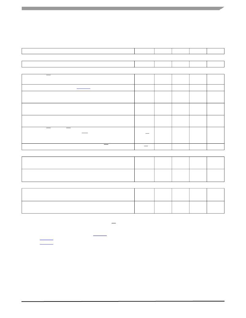
�MC33910BAC� /� MC34910BAC�
�ELECTRICAL� CHARACTERISTICS�
�DYNAMIC� ELECTRICAL� CHARACTERISTICS�
�Table� 34.� Dynamic� Electrical� Characteristics� (continued)�
�Characteristics� noted� under� conditions� 5.5� V� ≤� V� SUP� ≤� 18� V,� -40°C� ≤� T� A� ≤� 125°C� for� the� 33910� and� -40°C� ≤� T� A� ≤� 85°C� for� the�
�34910,� unless� otherwise� noted.� Typical� values� noted� reflect� the� approximate� parameter� mean� at� T� A� =� 25°C� under� nominal�
�conditions,� unless� otherwise� noted.�
�Characteristic�
�Symbol�
�Min�
�Typ�
�Max�
�Unit�
�L1� INPUT�
�Wake-up� Filter� Time�
�t� WUF�
�8.0�
�20�
�38�
�μ� s�
�STATE� MACHINE� TIMING�
�Delay� Between� CS� LOW-to-HIGH� Transition� (at� End� of� SPI� Stop� Command)�
�and� Stop� Mode� Activation� (107)�
��t� STOP�
�t� NR� TOUT�
�–�
�110�
�–�
�150�
�5.0�
�205�
�μ� s�
�ms�
�Delay� Between� SPI� Command� and� HS� Turn� On� (108)�
�t� S-� ON�
�μ� s�
�9.0� V� <� V� SUP� <� 27� V�
�Delay� Between� SPI� Command� and� HS� Turn� Off� (108)�
�9.0� V� <� V� SUP� <� 27� V�
�t� S-� OFF�
�–�
�–�
�–�
�–�
�10�
�10�
�μ� s�
�Delay� Between� Normal� Request� and� Normal� Mode� After� a� Watchdog� Trigger�
�Command� (Normal� Request� mode)� (107)�
�t� SNR2N�
�–�
�–�
�10�
�μ� s�
�Delay� Between� CS� Wake-up� (� CS� LOW� to� HIGH)� in� Stop� Mode� and:�
�μ� s�
�Normal� Request� mode,� VDD� ON� and� RST� HIGH�
�First� Accepted� SPI� Command�
�t� WUCS�
�t� WUSPI�
�9.0�
�90�
�15�
�—�
�80�
�N/A�
�Minimum� Time� Between� Rising� and� Falling� Edge� on� the� CS�
�t� 2CS�
�4.0�
�—�
�—�
�μ� s�
�LIN� PHYSICAL� LAYER:� DRIVER� CHARACTERISTICS� FOR� NORMAL� SLEW� RATE� -� 20.0� KBIT/SEC� (109)� ,� (110)�
�Duty� Cycle� 1:� D1� =� t� BUS_REC(MIN)� /(2� x� t� BIT� ),� t� BIT� =� 50� μs�
�7.0� V� ≤� V� SUP� ≤� 18� V�
�Duty� Cycle� 2:� D2� =� t� BUS_REC(MAX)� /(2� x� t� BIT� ),� t� BIT� =� 50� μs�
�7.6� V� ≤� V� SUP� ≤� 18� V�
�D1�
�D2�
�0.396�
�—�
�—�
�—�
�—�
�0.581�
�LIN� PHYSICAL� LAYER:� DRIVER� CHARACTERISTICS� FOR� SLOW� SLEW� RATE� -� 10.4�
��Duty� Cycle� 3:� D3� =� t� BUS_REC(MIN)� /(2� x� t� BIT� ),� t� BIT� =� 96� μs�
�7.0� V� ≤� V� SUP� ≤� 18� V�
�Duty� Cycle� 4:� D4� =� t� BUS_REC(MAX)� /(2� x� t� BIT� ),� t� BIT� =� 96� μs�
�7.6� V� ≤� V� SUP� ≤� 18� V�
�D3�
�D4�
�0.417�
�—�
�—�
�—�
�—�
�0.590�
�μ� s�
�μ� s�
�Notes�
�107.� This� parameter� is� guaranteed� by� process� monitoring� but,� not� production� tested.�
�108.� Delay� between� turn� on� or� off� command� (rising� edge� on� CS)� and� HS� ON� or� OFF,� excluding� rise� or� fall� time� due� to� external� load.�
�109.� Bus� load� R� BUS� and� C� BUS� 1.0� nF� /� 1.0� k� Ω� ,� 6.8� nF� /� 660� Ω� ,� 10� nF� /� 500� Ω� .� Measurement� thresholds:� 50%� of� TXD� signal� to� LIN� signal�
����33910�
�Analog� Integrated� Circuit� Device� Data�
�Freescale� Semiconductor�
�60�
�相关PDF资料 |
PDF描述 |
|---|---|
| 21020-0057 | CABLE FLAT FLEX 4" .50MM 6 POS |
| VE-B5W-EW | CONVERTER MOD DC/DC 5.5V 100W |
| A4973SB-T | IC PWM MOTOR DVR FULL 16DIP |
| MC33910BACR2 | IC SYSTEM BASIS CHIP 32LQFP |
| VE-B5V-EW | CONVERTER MOD DC/DC 5.8V 100W |
相关代理商/技术参数 |
参数描述 |
|---|---|
| MC33910G5ACR2 | 功能描述:LIN 收发器 SBC LIN 2.5G Low end RoHS:否 制造商:NXP Semiconductors 工作电源电压: 电源电流: 最大工作温度: 封装 / 箱体:SO-8 |
| MC33911BAC | 功能描述:LIN 收发器 SBC LIN2G MEDIUM END RoHS:否 制造商:NXP Semiconductors 工作电源电压: 电源电流: 最大工作温度: 封装 / 箱体:SO-8 |
| MC33911BACR2 | 功能描述:LIN 收发器 SBC LIN2G MEDIUM END RoHS:否 制造商:NXP Semiconductors 工作电源电压: 电源电流: 最大工作温度: 封装 / 箱体:SO-8 |
| MC33911G5AC | 功能描述:LIN 收发器 SBC LIN 2.5G Medium end RoHS:否 制造商:NXP Semiconductors 工作电源电压: 电源电流: 最大工作温度: 封装 / 箱体:SO-8 |
| MC33911G5ACR2 | 功能描述:LIN 收发器 SBC LIN 2.5G Medium end RoHS:否 制造商:NXP Semiconductors 工作电源电压: 电源电流: 最大工作温度: 封装 / 箱体:SO-8 |
发布紧急采购,3分钟左右您将得到回复。