- 您现在的位置:买卖IC网 > PDF目录45211 > MC68307PU16 (MOTOROLA INC) 16-BIT, 16.67 MHz, MICROCONTROLLER, PQFP100 PDF资料下载
参数资料
| 型号: | MC68307PU16 |
| 厂商: | MOTOROLA INC |
| 元件分类: | 微控制器/微处理器 |
| 英文描述: | 16-BIT, 16.67 MHz, MICROCONTROLLER, PQFP100 |
| 封装: | TQFP-100 |
| 文件页数: | 234/264页 |
| 文件大小: | 949K |
| 代理商: | MC68307PU16 |
第1页第2页第3页第4页第5页第6页第7页第8页第9页第10页第11页第12页第13页第14页第15页第16页第17页第18页第19页第20页第21页第22页第23页第24页第25页第26页第27页第28页第29页第30页第31页第32页第33页第34页第35页第36页第37页第38页第39页第40页第41页第42页第43页第44页第45页第46页第47页第48页第49页第50页第51页第52页第53页第54页第55页第56页第57页第58页第59页第60页第61页第62页第63页第64页第65页第66页第67页第68页第69页第70页第71页第72页第73页第74页第75页第76页第77页第78页第79页第80页第81页第82页第83页第84页第85页第86页第87页第88页第89页第90页第91页第92页第93页第94页第95页第96页第97页第98页第99页第100页第101页第102页第103页第104页第105页第106页第107页第108页第109页第110页第111页第112页第113页第114页第115页第116页第117页第118页第119页第120页第121页第122页第123页第124页第125页第126页第127页第128页第129页第130页第131页第132页第133页第134页第135页第136页第137页第138页第139页第140页第141页第142页第143页第144页第145页第146页第147页第148页第149页第150页第151页第152页第153页第154页第155页第156页第157页第158页第159页第160页第161页第162页第163页第164页第165页第166页第167页第168页第169页第170页第171页第172页第173页第174页第175页第176页第177页第178页第179页第180页第181页第182页第183页第184页第185页第186页第187页第188页第189页第190页第191页第192页第193页第194页第195页第196页第197页第198页第199页第200页第201页第202页第203页第204页第205页第206页第207页第208页第209页第210页第211页第212页第213页第214页第215页第216页第217页第218页第219页第220页第221页第222页第223页第224页第225页第226页第227页第228页第229页第230页第231页第232页第233页当前第234页第235页第236页第237页第238页第239页第240页第241页第242页第243页第244页第245页第246页第247页第248页第249页第250页第251页第252页第253页第254页第255页第256页第257页第258页第259页第260页第261页第262页第263页第264页
Bus Operation
MOTOROLA
MC68307 USER’S MANUAL
3-33
increases performance by observing timing parameters related to the system clock fre-
quency without being completely synchronous with that clock. A memory array designed to
operate with a particular frequency processor but not driven by the processor clock is a com-
mon example of a pseudo-asynchronous device.
The designer of a fully asynchronous system can make no assumptions about address
setup time, which could be used to improve performance. With the system clock frequency
known, the slave device can be designed to decode the address bus before recognizing an
address strobe. Parameter #11 (refer to Section 11.7 AC Electrical Specifications—Read
and Write Cycles (VCC = 5.0V
± 0.5V or 3.3Vdc ± 0.3V; GND = 0Vdc; TA = TL to TH)
(see Figure 11-3 and Figure 11-4)) specifies the minimum time before address strobe dur-
ing which the address is valid.
In a pseudo-asynchronous system, timing specifications allow DTACK to be asserted for a
read cycle before the data from a slave device is valid. The length of time that DTACK may
precede data is specified as parameter #31. This parameter must be met to ensure the valid-
ity of the data latched into the processor. No maximum time is specified from the assertion
of AS to the assertion of DTACK. During this unlimited time, the processor inserts wait
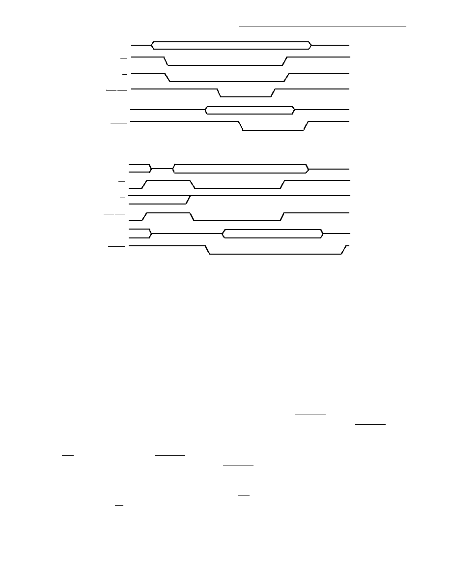
cycles in one-clock-period increments until DTACK is recognized. Figure 3-33 shows the
important timing parameters for a pseudo-asynchronous read cycle.
During a write cycle, after the processor asserts AS but before driving the data bus, the pro-
cessor drives R/W low. Parameter #55 specifies the minimum time between the transition
Figure 3-30. Fully Asynchronous Write Cycle
Figure 3-31. Fully Asynchronous Read Cycle
ADDR
AS
R/W
UDS/LDS
DATA
DTACK
ADDR
AS
R/W
UDS/LDS
DATA
DTACK
AS
R/W
DTACK
UDS/LDS
DATA
ADDR
AS
R/W
UDS/LDS
DATA
DTACK
相关PDF资料 |
PDF描述 |
|---|---|
| MC68307PU16V | 16-BIT, 16.67 MHz, MICROCONTROLLER, PQFP100 |
| MC68307FG16 | 16-BIT, 16.67 MHz, MICROCONTROLLER, PQFP100 |
| MC68322FT16 | 16-BIT, 16.667 MHz, RISC PROCESSOR, PQFP160 |
| MC68331CFC20B1 | 32-BIT, 20 MHz, MICROCONTROLLER, PQFP132 |
| MC68331CPV20B1 | 32-BIT, 20 MHz, MICROCONTROLLER, PQFP144 |
相关代理商/技术参数 |
参数描述 |
|---|---|
| MC68307UM | 制造商:MOTOROLA 制造商全称:Motorola, Inc 功能描述:Technical Summary Integrated Multiple-Bus Processor |
| MC68307V | 制造商:MOTOROLA 制造商全称:Motorola, Inc 功能描述:Technical Summary Integrated Multiple-Bus Processor |
| MC68322 | 制造商:MOTOROLA 制造商全称:Motorola, Inc 功能描述:Integrated Printer Processor |
| MC68322AD | 制造商:MOTOROLA 制造商全称:Motorola, Inc 功能描述:Integrated Printer Processor |
| MC68322FT20 | 制造商:Rochester Electronics LLC 功能描述:- Bulk |
发布紧急采购,3分钟左右您将得到回复。