- 您现在的位置:买卖IC网 > PDF目录10963 > MC705JP7CPE (Freescale Semiconductor)IC MCU 8BIT 224 BYTES RAM 28PDIP PDF资料下载
参数资料
| 型号: | MC705JP7CPE |
| 厂商: | Freescale Semiconductor |
| 文件页数: | 162/164页 |
| 文件大小: | 0K |
| 描述: | IC MCU 8BIT 224 BYTES RAM 28PDIP |
| 标准包装: | 13 |
| 系列: | HC05 |
| 核心处理器: | HC05 |
| 芯体尺寸: | 8-位 |
| 速度: | 2.1MHz |
| 连通性: | SIO |
| 外围设备: | POR,温度传感器,WDT |
| 输入/输出数: | 22 |
| 程序存储器容量: | 6KB(6K x 8) |
| 程序存储器类型: | OTP |
| RAM 容量: | 224 x 8 |
| 电压 - 电源 (Vcc/Vdd): | 2.7 V ~ 5.5 V |
| 数据转换器: | A/D 4x12b |
| 振荡器型: | 内部 |
| 工作温度: | -40°C ~ 85°C |
| 封装/外壳: | 28-DIP(0.600",15.24mm) |
| 包装: | 管件 |
第1页第2页第3页第4页第5页第6页第7页第8页第9页第10页第11页第12页第13页第14页第15页第16页第17页第18页第19页第20页第21页第22页第23页第24页第25页第26页第27页第28页第29页第30页第31页第32页第33页第34页第35页第36页第37页第38页第39页第40页第41页第42页第43页第44页第45页第46页第47页第48页第49页第50页第51页第52页第53页第54页第55页第56页第57页第58页第59页第60页第61页第62页第63页第64页第65页第66页第67页第68页第69页第70页第71页第72页第73页第74页第75页第76页第77页第78页第79页第80页第81页第82页第83页第84页第85页第86页第87页第88页第89页第90页第91页第92页第93页第94页第95页第96页第97页第98页第99页第100页第101页第102页第103页第104页第105页第106页第107页第108页第109页第110页第111页第112页第113页第114页第115页第116页第117页第118页第119页第120页第121页第122页第123页第124页第125页第126页第127页第128页第129页第130页第131页第132页第133页第134页第135页第136页第137页第138页第139页第140页第141页第142页第143页第144页第145页第146页第147页第148页第149页第150页第151页第152页第153页第154页第155页第156页第157页第158页第159页第160页第161页当前第162页第163页第164页
SIOP Registers
MC68HC705JJ7 MC68HC705JP7 Advance Information Data Sheet, Rev. 4.1
Freescale Semiconductor
97
9.2.2 Serial Data Input (SDI)
The SDI pin becomes an input as soon as the SIOP subsystem is enabled. New data is presented to the
SDI pin on the falling edge of SCK. Valid data must be present at least 100 nanoseconds before the rising
edge of SCK and remain valid for 100 nanoseconds after the rising edge of SCK. See Figure 9-3.
9.2.3 Serial Data Output (SDO)
The SDO pin becomes an output as soon as the SIOP subsystem is enabled. The state of the PB5/SDO
pin reflects the value of the first bit received on the previous transmission. Prior to enabling the SIOP, the
PB5/SDO can be initialized to determine the beginning state. While SIOP is enabled, the port B logic
cannot be used as a standard output since that pin is connected to the last stage of the SIOP serial shift
register. A control bit (LSBF) is included in the SCR to allow the data to be transmitted in either the MSB
first format or the LSB first format.
The first data bit will be shifted out to the SDO pin on the first falling edge of the SCK. The remaining data
bits will be shifted out to the SDI pin on subsequent falling edges of SCK. The SDO pin will present valid
data at least 100 nanoseconds before the rising edge of the SCK and remain valid for 100 nanoseconds
after the rising edge of SCK. See Figure 9-3.
9.3 SIOP Registers
The SIOP is programmed and controlled by the SIOP control register (SCR) located at address $000A,
the SIOP status register (SSR) located at address $000B, and the SIOP data register (SDR) located at
address $000C.
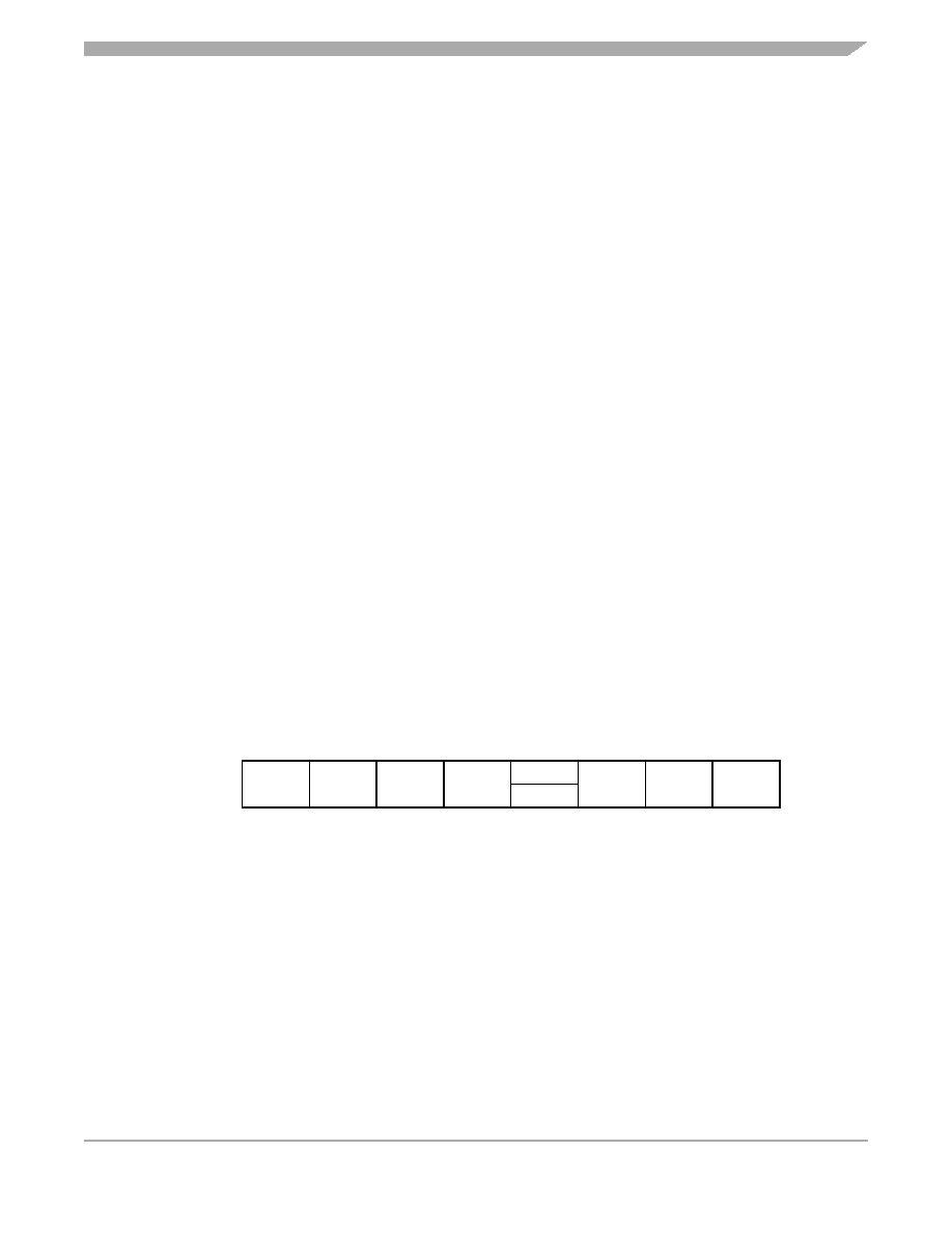
9.3.1 SIOP Control Register (SCR)
The SIOP control register (SCR) is located at address $000A and contains seven control bits and a
write-only reset of the interrupt flag. Figure 9-4 shows the position of each bit in the register and indicates
the value of each bit after reset.
SPIE — Serial Peripheral Interrupt Enable Bit
The SPIE bit enables the SIOP to generate an interrupt whenever the SPIF flag bit in the SSR is set.
Clearing the SPIE bit will not affect the state of the SPIF flag bit and will not terminate a serial interrupt
once the interrupt sequence has started. Reset clears the SPIE bit.
1 = Serial interrupt enabled
0 = Serial interrupt disabled
NOTE
If the SPIE bit is cleared just after the serial interrupt sequence has started
(for instance, the CPU status is being stacked), then the CPU will be unable
Address:
$000A
Bit 7
654321
Bit 0
Read:
SPIE
SPE
LSBF
MSTR
0
CPHA
SPR1
SPR0
Write:
SPIR
Reset:
00000000
Figure 9-4. SIOP Control Register (SCR)
相关PDF资料 |
PDF描述 |
|---|---|
| S912XEG128J2MAA | MCU 16BIT 128K FLASH 16K 80QFP |
| MC9S12XD64MAA | IC MCU 16BIT 64K FLASH 80-QFP |
| MC56F8322VFAER2 | IC HYBRID CTRLR 16BIT 48-LQFP |
| MCF5207CVM166J | IC MCU 32BIT RISC 144-MAPBGA |
| MC68908GZ16MFJE | IC MCU 8BIT 16K FLASH 32-LQFP |
相关代理商/技术参数 |
参数描述 |
|---|---|
| MC705JP7CPE | 制造商:Freescale Semiconductor 功能描述:IC 8BIT MCU 68HC05 2.1MHZ DIP-28 |
| MC705K1CP | 制造商:Motorola Inc 功能描述:16 PIN DIP INTEGRATED CIRCUIT |
| MC705L16CFUE | 功能描述:8位微控制器 -MCU 8B MCU W/ EPROM RoHS:否 制造商:Silicon Labs 核心:8051 处理器系列:C8051F39x 数据总线宽度:8 bit 最大时钟频率:50 MHz 程序存储器大小:16 KB 数据 RAM 大小:1 KB 片上 ADC:Yes 工作电源电压:1.8 V to 3.6 V 工作温度范围:- 40 C to + 105 C 封装 / 箱体:QFN-20 安装风格:SMD/SMT |
| MC705P6ACDWE | 功能描述:8位微控制器 -MCU MCU 176 BYTES RAM A/D RoHS:否 制造商:Silicon Labs 核心:8051 处理器系列:C8051F39x 数据总线宽度:8 bit 最大时钟频率:50 MHz 程序存储器大小:16 KB 数据 RAM 大小:1 KB 片上 ADC:Yes 工作电源电压:1.8 V to 3.6 V 工作温度范围:- 40 C to + 105 C 封装 / 箱体:QFN-20 安装风格:SMD/SMT |
| MC705P6ACDWE | 制造商:Freescale Semiconductor 功能描述:8-Bit Microcontroller IC |
发布紧急采购,3分钟左右您将得到回复。