- 您现在的位置:买卖IC网 > PDF目录45285 > MC9328MX21VH (FREESCALE SEMICONDUCTOR INC) 266 MHz, MICROPROCESSOR, PBGA289 PDF资料下载
参数资料
| 型号: | MC9328MX21VH |
| 厂商: | FREESCALE SEMICONDUCTOR INC |
| 元件分类: | 微控制器/微处理器 |
| 英文描述: | 266 MHz, MICROPROCESSOR, PBGA289 |
| 封装: | 17 X 17 MM, 1.45 MM HEIGHT, 0.80 MM PITCH, MAPBGA-289 |
| 文件页数: | 26/106页 |
| 文件大小: | 1932K |
| 代理商: | MC9328MX21VH |
第1页第2页第3页第4页第5页第6页第7页第8页第9页第10页第11页第12页第13页第14页第15页第16页第17页第18页第19页第20页第21页第22页第23页第24页第25页当前第26页第27页第28页第29页第30页第31页第32页第33页第34页第35页第36页第37页第38页第39页第40页第41页第42页第43页第44页第45页第46页第47页第48页第49页第50页第51页第52页第53页第54页第55页第56页第57页第58页第59页第60页第61页第62页第63页第64页第65页第66页第67页第68页第69页第70页第71页第72页第73页第74页第75页第76页第77页第78页第79页第80页第81页第82页第83页第84页第85页第86页第87页第88页第89页第90页第91页第92页第93页第94页第95页第96页第97页第98页第99页第100页第101页第102页第103页第104页第105页第106页
MC9328MX21 Product Preview, Rev. 1.1
26
Freescale Semiconductor
Specifications
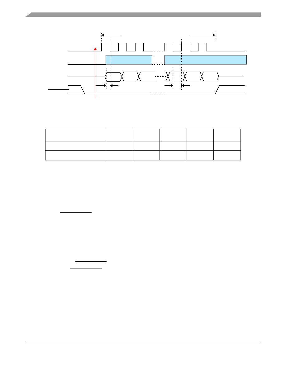
Figure 9. BMI Drives Clock, MMD Write BMI Timing
(MASTER_MODE_SEL=0, MMD_MODE_SEL=1, MMD_CLKOUT=1)
Note: The BMI_CLK/CS can only be up to 30Mhz if BMI latch data at the falling edge and can be up to 36Mhz (double as max
data pad speed) if BMI latch data at the next rising edge.
Note: Tds1 is the receive data setup time when BMI latch data at the falling edge.
Note: Tds2 is the receive data setup time when BMI latch data at the next rising edge.
3.8.2
Connecting BMI to External Bus Master Devices
In this mode both MASTER_SEL bit and MMD_MODE_SEL bit are cleared and the MMD_CLKOUT
bit is no useful. BMI_WRITE and BMI_CLK/CS are input signals driving by the external bus master. The
Output signal BMI_READ_REQ can be used as an interrupt signal to inform external bus master that data
is ready in the BMI TxFIFO for a read access. The external bus master can write data to the BMI RxFIFO
anytime since the CPU or DMA can move data out from RxFIFO much faster than the BMI interface. An
overflow interrupt is generated if RxFIFO overflow is detected. Once this happens, the new coming data
is ignored.
Each falling edge of BMI_CLK/CS will determine if the current cycle is read or write cycle. It drives data
and enables data out if BMI_WRITE is logic high. The D_EN signal remains active only while BMI_CLK/
CS is logic low and BMI_WRITE is logic high.
Each rising edge of BMI_CLK/CS will determine if data should be latched to RxFIFO from the data bus.
Table 15. MMD Write BMI Timing Table when BMI Drives Clock
Item
Symbol
Minimum
Typical
Maximum
Unit
receive data setup time1
Tds1
14
–
ns
receive data setup time2
Tds2
14
–
ns
Can be asserted any time
BMI_CLK/CS
BMI_READ_REQ
BMI_WRITE
BMI_D[15:0]
RxD1
RxD2
Last RxD
Tds1
Tds2
A 1 is written to READ bit of control register
Total has COUNT+1 clocks in one burst
相关PDF资料 |
PDF描述 |
|---|---|
| MC9328MX21CVG | 266 MHz, MICROPROCESSOR, PBGA289 |
| MC9328MX21CVH | 266 MHz, MICROPROCESSOR, PBGA289 |
| MC9328MX21DVH | 266 MHz, MICROPROCESSOR, PBGA289 |
| MC9328MX21DVG | 266 MHz, MICROPROCESSOR, PBGA289 |
| MC9328MXLCVM15R2 | 32-BIT, 150 MHz, RISC PROCESSOR, PBGA256 |
相关代理商/技术参数 |
参数描述 |
|---|---|
| MC9328MX21VK | 功能描述:处理器 - 专门应用 DB I.MX21 PB-FR RoHS:否 制造商:Freescale Semiconductor 类型:Multimedia Applications 核心:ARM Cortex A9 处理器系列:i.MX6 数据总线宽度:32 bit 最大时钟频率:1 GHz 指令/数据缓存: 数据 RAM 大小:128 KB 数据 ROM 大小: 工作电源电压: 最大工作温度:+ 95 C 安装风格:SMD/SMT 封装 / 箱体:MAPBGA-432 |
| MC9328MX21VK | 制造商:Freescale Semiconductor 功能描述:Microprocessor |
| MC9328MX21VKR2 | 功能描述:处理器 - 专门应用 DB I.MX21 PB-FR RoHS:否 制造商:Freescale Semiconductor 类型:Multimedia Applications 核心:ARM Cortex A9 处理器系列:i.MX6 数据总线宽度:32 bit 最大时钟频率:1 GHz 指令/数据缓存: 数据 RAM 大小:128 KB 数据 ROM 大小: 工作电源电压: 最大工作温度:+ 95 C 安装风格:SMD/SMT 封装 / 箱体:MAPBGA-432 |
| MC9328MX21VM | 功能描述:处理器 - 专门应用 DB I.MX21 17X17 PB-FR RoHS:否 制造商:Freescale Semiconductor 类型:Multimedia Applications 核心:ARM Cortex A9 处理器系列:i.MX6 数据总线宽度:32 bit 最大时钟频率:1 GHz 指令/数据缓存: 数据 RAM 大小:128 KB 数据 ROM 大小: 工作电源电压: 最大工作温度:+ 95 C 安装风格:SMD/SMT 封装 / 箱体:MAPBGA-432 |
| MC9328MX21VM | 制造商:Freescale Semiconductor 功能描述:Microprocessor |
发布紧急采购,3分钟左右您将得到回复。