- 您现在的位置:买卖IC网 > PDF目录45285 > MC9328MX21VH (FREESCALE SEMICONDUCTOR INC) 266 MHz, MICROPROCESSOR, PBGA289 PDF资料下载
参数资料
| 型号: | MC9328MX21VH |
| 厂商: | FREESCALE SEMICONDUCTOR INC |
| 元件分类: | 微控制器/微处理器 |
| 英文描述: | 266 MHz, MICROPROCESSOR, PBGA289 |
| 封装: | 17 X 17 MM, 1.45 MM HEIGHT, 0.80 MM PITCH, MAPBGA-289 |
| 文件页数: | 85/106页 |
| 文件大小: | 1932K |
| 代理商: | MC9328MX21VH |
第1页第2页第3页第4页第5页第6页第7页第8页第9页第10页第11页第12页第13页第14页第15页第16页第17页第18页第19页第20页第21页第22页第23页第24页第25页第26页第27页第28页第29页第30页第31页第32页第33页第34页第35页第36页第37页第38页第39页第40页第41页第42页第43页第44页第45页第46页第47页第48页第49页第50页第51页第52页第53页第54页第55页第56页第57页第58页第59页第60页第61页第62页第63页第64页第65页第66页第67页第68页第69页第70页第71页第72页第73页第74页第75页第76页第77页第78页第79页第80页第81页第82页第83页第84页当前第85页第86页第87页第88页第89页第90页第91页第92页第93页第94页第95页第96页第97页第98页第99页第100页第101页第102页第103页第104页第105页第106页
MC9328MX21 Product Preview, Rev. 1.1
8
Freescale Semiconductor
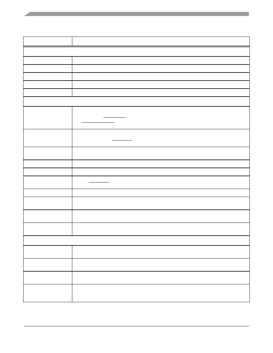
Signal Descriptions
CMOS Sensor Interface
CSI_D [7:0]
Sensor port data
CSI_MCLK
Sensor port master clock
CSI_VSYNC
Sensor port vertical sync
CSI_HSYNC
Sensor port horizontal sync
CSI_PIXCLK
Sensor port data latch clock
LCD Controller
LD [17:0]
LCD Data Bus—All LCD signals are driven low after reset and when LCD is off. LD[15:0] signals
are multiplexed with SLCDC1_DAT[15:0] from SLCDC1 and BMI_D[15:0]. LD[17] signal is
multiplexed with BMI_WRITE of BMI. LD[16] signal is multiplexed with BMI_READ_REQ of BMI
and EXT_DMAGRANT signals.
FLM_VSYNC
(or simply referred
to as VSYNC)
Frame Sync or Vsync—This signal also serves as the clock signal output for gate
driver (dedicated signal SPS for Sharp panel HR-TFT). This signal is multiplexed with
BMI_RXF_FULL and BMI_WAIT of the BMI.
LP_HSYNC (or simply
referred to as HSYNC)
Line Pulse or HSync
LSCLK
Shift Clock. This signal is multiplexed with the BMI_CLK_CS from BMI.
OE_ACD
Alternate Crystal Direction/Output Enable.
CONTRAST
This signal is used to control the LCD bias voltage as contrast control. This signal is multiplexed
with the BMI_READ from BMI.
SPL_SPR
Sampling start signal for left and right scanning. This signal is multiplexed with the SLCDC1_CLK.
PS
Control signal output for source driver (Sharp panel dedicated signal). This signal is multiplexed
with the SLCDC1_CS.
CLS
Start signal output for gate driver. This signal is invert version of PS (Sharp panel dedicated
signal). This signal is multiplexed with the SLCDC1_RS.
REV
Signal for common electrode driving signal preparation (Sharp panel dedicated signal). This signal
is multiplexed with SLCDC1_D0.
Smart LCD Controller
SLCDC1_CLK
SLCDC Clock output signal. This signal is multiplexed and available at 2 alternate locations. These
are SPL_SPR and SD2_CLK signals of LCDC and SD2, respectively.
SLCDC1_CS
SLCDC Chip Select output signal. This signal is multiplexed and available at 2 alternate signal
locations. These are PS and SD2_CMD signals of LCDC and SD2, respectively.
SLCDC1_RS
SLCDC Register Select output signal. This signal is multiplexed and available at 2 alternate signal
locations. These are CLS and SD2_D3 signals of LCDC and SD2, respectively.
SLCDC1_D0
SLCDC serial data output signal. This signal is multiplexed and available at 2 alternate signal
locations. These are and REV and SD2_D2 signals of LCDC and SD2, respectively. This signal is
inactive when a parallel data interface is used.
Table 2. i.MX21 Signal Descriptions (Continued)
Signal Name
Function/Notes
相关PDF资料 |
PDF描述 |
|---|---|
| MC9328MX21CVG | 266 MHz, MICROPROCESSOR, PBGA289 |
| MC9328MX21CVH | 266 MHz, MICROPROCESSOR, PBGA289 |
| MC9328MX21DVH | 266 MHz, MICROPROCESSOR, PBGA289 |
| MC9328MX21DVG | 266 MHz, MICROPROCESSOR, PBGA289 |
| MC9328MXLCVM15R2 | 32-BIT, 150 MHz, RISC PROCESSOR, PBGA256 |
相关代理商/技术参数 |
参数描述 |
|---|---|
| MC9328MX21VK | 功能描述:处理器 - 专门应用 DB I.MX21 PB-FR RoHS:否 制造商:Freescale Semiconductor 类型:Multimedia Applications 核心:ARM Cortex A9 处理器系列:i.MX6 数据总线宽度:32 bit 最大时钟频率:1 GHz 指令/数据缓存: 数据 RAM 大小:128 KB 数据 ROM 大小: 工作电源电压: 最大工作温度:+ 95 C 安装风格:SMD/SMT 封装 / 箱体:MAPBGA-432 |
| MC9328MX21VK | 制造商:Freescale Semiconductor 功能描述:Microprocessor |
| MC9328MX21VKR2 | 功能描述:处理器 - 专门应用 DB I.MX21 PB-FR RoHS:否 制造商:Freescale Semiconductor 类型:Multimedia Applications 核心:ARM Cortex A9 处理器系列:i.MX6 数据总线宽度:32 bit 最大时钟频率:1 GHz 指令/数据缓存: 数据 RAM 大小:128 KB 数据 ROM 大小: 工作电源电压: 最大工作温度:+ 95 C 安装风格:SMD/SMT 封装 / 箱体:MAPBGA-432 |
| MC9328MX21VM | 功能描述:处理器 - 专门应用 DB I.MX21 17X17 PB-FR RoHS:否 制造商:Freescale Semiconductor 类型:Multimedia Applications 核心:ARM Cortex A9 处理器系列:i.MX6 数据总线宽度:32 bit 最大时钟频率:1 GHz 指令/数据缓存: 数据 RAM 大小:128 KB 数据 ROM 大小: 工作电源电压: 最大工作温度:+ 95 C 安装风格:SMD/SMT 封装 / 箱体:MAPBGA-432 |
| MC9328MX21VM | 制造商:Freescale Semiconductor 功能描述:Microprocessor |
发布紧急采购,3分钟左右您将得到回复。