- 您现在的位置:买卖IC网 > PDF目录45285 > MC9328MX21VH (FREESCALE SEMICONDUCTOR INC) 266 MHz, MICROPROCESSOR, PBGA289 PDF资料下载
参数资料
| 型号: | MC9328MX21VH |
| 厂商: | FREESCALE SEMICONDUCTOR INC |
| 元件分类: | 微控制器/微处理器 |
| 英文描述: | 266 MHz, MICROPROCESSOR, PBGA289 |
| 封装: | 17 X 17 MM, 1.45 MM HEIGHT, 0.80 MM PITCH, MAPBGA-289 |
| 文件页数: | 63/106页 |
| 文件大小: | 1932K |
| 代理商: | MC9328MX21VH |
第1页第2页第3页第4页第5页第6页第7页第8页第9页第10页第11页第12页第13页第14页第15页第16页第17页第18页第19页第20页第21页第22页第23页第24页第25页第26页第27页第28页第29页第30页第31页第32页第33页第34页第35页第36页第37页第38页第39页第40页第41页第42页第43页第44页第45页第46页第47页第48页第49页第50页第51页第52页第53页第54页第55页第56页第57页第58页第59页第60页第61页第62页当前第63页第64页第65页第66页第67页第68页第69页第70页第71页第72页第73页第74页第75页第76页第77页第78页第79页第80页第81页第82页第83页第84页第85页第86页第87页第88页第89页第90页第91页第92页第93页第94页第95页第96页第97页第98页第99页第100页第101页第102页第103页第104页第105页第106页
MC9328MX21 Product Preview, Rev. 1.1
6
Freescale Semiconductor
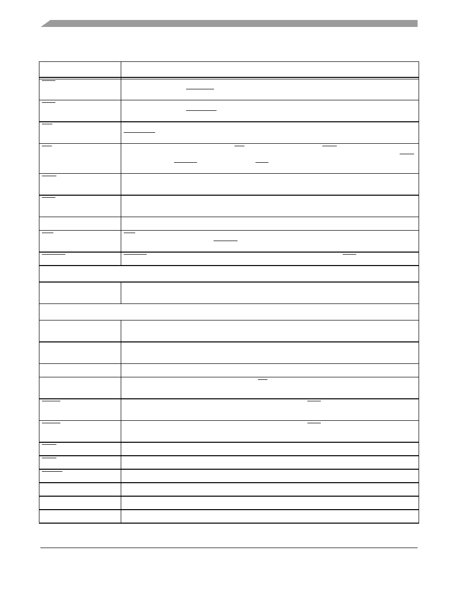
Signal Descriptions
EB2
Byte Strobe—Active low external enable byte signal that controls D [15:8], shared with SDRAM
DQM2 and PCMCIA PC_REG.
EB3
LSB Byte Strobe—Active low external enable byte signal that controls D [7:0], shared with SDRAM
DQM3 and PCMCIA PC_IORD.
OE
Memory Output Enable—Active low output enables external data bus, shared with PCMCIA
PC_IOWR.
CS [5:0]
Chip Select—The chip select signals CS [3:2] are multiplexed with CSD [1:0] and are selected by
the Function Multiplexing Control Register (FMCR) in the System Control chapter. By default CSD
[1:0] is selected. DTACK is multiplexed with CS4.
ECB
Active low input signal sent by flash device to the EIM whenever the flash device must terminate an
on-going burst sequence and initiate a new (long first access) burst sequence.
LBA
Active low signal sent by flash device causing the external burst device to latch the starting burst
address.
BCLK
Clock signal sent to external synchronous memories (such as burst flash) during burst mode.
RW
RW signal—Indicates whether external access is a read (high) or write (low) cycle. This signal is
also shared with the PCMCIA PC_WE.
DTACK
DTACK signal—External input data acknowledge signal, multiplexed with CS4.
Bootstrap
BOOT [3:0]
System Boot Mode Select—The operational system boot mode of the i.MX21 upon system reset is
determined by the settings of these pins.
SDRAM Controller
SDBA [4:0]
SDRAM non-interleave mode bank address signals. These signals are multiplexed with address
signals A[20:16].
SDIBA [3:0]
SDRAM interleave addressing mode bank address signals. These signals are multiplexed with
address signals A[24:21].
MA [11:0]
SDRAM address signals. MA[9:0] are multiplexed with address signals A[10:1].
DQM [3:0]
SDRAM data qualifier mask multiplexed with EB[3:0]. DQM3 corresponds to D[31:24], DQM2
corresponds to D[23:16], DQM1 corresponds to D[15:8], and DQM0 corresponds to D[7:0].
CSD0
SDRAM Chip Select signal. This signal is multiplexed with the CS2 signal. This signal is selectable
by programming the Function Multiplexing Control Register in the System Control chapter.
CSD1
SDRAM Chip Select signal. This signal is multiplexed with the CS3 signal. This signal is selectable
by programming the Function Multiplexing Control Register in the System Control chapter.
RAS
SDRAM Row Address Select signal
CAS
SDRAM Column Address Select signal
SDWE
SDRAM Write Enable signal
SDCKE0
SDRAM Clock Enable 0
SDCKE1
SDRAM Clock Enable 1
SDCLK
SDRAM Clock
Table 2. i.MX21 Signal Descriptions (Continued)
Signal Name
Function/Notes
相关PDF资料 |
PDF描述 |
|---|---|
| MC9328MX21CVG | 266 MHz, MICROPROCESSOR, PBGA289 |
| MC9328MX21CVH | 266 MHz, MICROPROCESSOR, PBGA289 |
| MC9328MX21DVH | 266 MHz, MICROPROCESSOR, PBGA289 |
| MC9328MX21DVG | 266 MHz, MICROPROCESSOR, PBGA289 |
| MC9328MXLCVM15R2 | 32-BIT, 150 MHz, RISC PROCESSOR, PBGA256 |
相关代理商/技术参数 |
参数描述 |
|---|---|
| MC9328MX21VK | 功能描述:处理器 - 专门应用 DB I.MX21 PB-FR RoHS:否 制造商:Freescale Semiconductor 类型:Multimedia Applications 核心:ARM Cortex A9 处理器系列:i.MX6 数据总线宽度:32 bit 最大时钟频率:1 GHz 指令/数据缓存: 数据 RAM 大小:128 KB 数据 ROM 大小: 工作电源电压: 最大工作温度:+ 95 C 安装风格:SMD/SMT 封装 / 箱体:MAPBGA-432 |
| MC9328MX21VK | 制造商:Freescale Semiconductor 功能描述:Microprocessor |
| MC9328MX21VKR2 | 功能描述:处理器 - 专门应用 DB I.MX21 PB-FR RoHS:否 制造商:Freescale Semiconductor 类型:Multimedia Applications 核心:ARM Cortex A9 处理器系列:i.MX6 数据总线宽度:32 bit 最大时钟频率:1 GHz 指令/数据缓存: 数据 RAM 大小:128 KB 数据 ROM 大小: 工作电源电压: 最大工作温度:+ 95 C 安装风格:SMD/SMT 封装 / 箱体:MAPBGA-432 |
| MC9328MX21VM | 功能描述:处理器 - 专门应用 DB I.MX21 17X17 PB-FR RoHS:否 制造商:Freescale Semiconductor 类型:Multimedia Applications 核心:ARM Cortex A9 处理器系列:i.MX6 数据总线宽度:32 bit 最大时钟频率:1 GHz 指令/数据缓存: 数据 RAM 大小:128 KB 数据 ROM 大小: 工作电源电压: 最大工作温度:+ 95 C 安装风格:SMD/SMT 封装 / 箱体:MAPBGA-432 |
| MC9328MX21VM | 制造商:Freescale Semiconductor 功能描述:Microprocessor |
发布紧急采购,3分钟左右您将得到回复。