- 您现在的位置:买卖IC网 > PDF目录10964 > MCHC705JJ7CPE (Freescale Semiconductor)IC MCU 8BIT 224 BYTES RAM 20PDIP PDF资料下载
参数资料
| 型号: | MCHC705JJ7CPE |
| 厂商: | Freescale Semiconductor |
| 文件页数: | 120/164页 |
| 文件大小: | 0K |
| 描述: | IC MCU 8BIT 224 BYTES RAM 20PDIP |
| 标准包装: | 18 |
| 系列: | HC05 |
| 核心处理器: | HC05 |
| 芯体尺寸: | 8-位 |
| 速度: | 2.1MHz |
| 连通性: | SIO |
| 外围设备: | POR,温度传感器,WDT |
| 输入/输出数: | 14 |
| 程序存储器容量: | 6KB(6K x 8) |
| 程序存储器类型: | OTP |
| RAM 容量: | 224 x 8 |
| 电压 - 电源 (Vcc/Vdd): | 2.7 V ~ 5.5 V |
| 数据转换器: | A/D 4x12b |
| 振荡器型: | 内部 |
| 工作温度: | -40°C ~ 85°C |
| 封装/外壳: | 20-DIP(0.300",7.62mm) |
| 包装: | 管件 |
第1页第2页第3页第4页第5页第6页第7页第8页第9页第10页第11页第12页第13页第14页第15页第16页第17页第18页第19页第20页第21页第22页第23页第24页第25页第26页第27页第28页第29页第30页第31页第32页第33页第34页第35页第36页第37页第38页第39页第40页第41页第42页第43页第44页第45页第46页第47页第48页第49页第50页第51页第52页第53页第54页第55页第56页第57页第58页第59页第60页第61页第62页第63页第64页第65页第66页第67页第68页第69页第70页第71页第72页第73页第74页第75页第76页第77页第78页第79页第80页第81页第82页第83页第84页第85页第86页第87页第88页第89页第90页第91页第92页第93页第94页第95页第96页第97页第98页第99页第100页第101页第102页第103页第104页第105页第106页第107页第108页第109页第110页第111页第112页第113页第114页第115页第116页第117页第118页第119页当前第120页第121页第122页第123页第124页第125页第126页第127页第128页第129页第130页第131页第132页第133页第134页第135页第136页第137页第138页第139页第140页第141页第142页第143页第144页第145页第146页第147页第148页第149页第150页第151页第152页第153页第154页第155页第156页第157页第158页第159页第160页第161页第162页第163页第164页
Port B
MC68HC705JJ7 MC68HC705JP7 Advance Information Data Sheet, Rev. 4.1
Freescale Semiconductor
59
PB0-PB7 — Port B Data Bits
These read/write bits are software programmable. Data direction of each bit is under the control of the
corresponding bit in data direction register B. Reset has no effect on port B data.
7.3.2 Data Direction Register B
The contents of the port B data direction register (DDRB) determine whether each port B pin is an input
or an output. Writing a logic 1 to a DDRB bit enables the output buffer for the associated port B pin. A
DDRB bit set to a logic 1 also disables the pulldown device for that pin. Writing a logic 0 to a DDRB bit
disables the output buffer for the associated port B pin. A reset initializes all DDRB bits to logic 0s,
configuring all port B pins as inputs.
DDRB7–DDRB0 — Port B Data Direction Bits
These read/write bits control port B data direction. Reset clears the bits DDRB7–DDRB0.
1 = Corresponding port B pin configured as output and pulldown device disabled
0 = Corresponding port B pin configured as input
7.3.3 Pulldown Register B
All port B pins can have software programmable pulldown devices enabled or disabled globally by the
SWPDI bit in the MOR. These pulldown devices are individually controlled by the write-only pulldown
register B (PDRB) shown in Figure 7-7. Clearing the PDIB7–PDIB0 bits in the PDRB turns on the pulldown
devices if the port B pin is an input. Reading the PDRB returns undefined results since it is a write-only
register. Reset clears the PDIB7–PDIB0 bits, which turns on all the port B pulldown devices.
PDIB7–PDIB0 — Port B Pulldown Inhibit Bits
Writing to these write-only bits controls the port B pulldown devices. Reading these pulldown register
B bits returns undefined data. Reset clears bits PDIB7–PDIB0.
1 = Corresponding port B pin pulldown device turned off
0 = Corresponding port B pin pulldown device turned on if pin has been programmed by the DDRB
to be an input
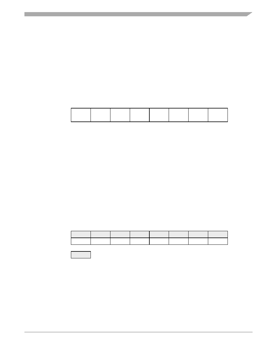
Address:
$0005
Bit 7
654321
Bit 0
Read:
DDRB7
DDRB6
DDRB5
DDRB4
DDRB3
DDRB2
DDRB1
DDRB0
Write:
Reset:
00000000
Figure 7-6. Data Direction Register B (DDRB)
Address:
$0011
Bit 7
654321
Bit 0
Read:
Write:
PDIB7
PDIB6
PDIB5
PDIB4
PDIB3
PDIB2
PDIB1
DIB0
Reset:
00000000
= Unimplemented
Figure 7-7. Pulldown Register B (PDRB)
相关PDF资料 |
PDF描述 |
|---|---|
| VI-B4L-IX-B1 | CONVERTER MOD DC/DC 28V 75W |
| VI-B4K-IW-B1 | CONVERTER MOD DC/DC 40V 100W |
| VI-B4J-IX-B1 | CONVERTER MOD DC/DC 36V 75W |
| VI-B4J-IW-B1 | CONVERTER MOD DC/DC 36V 100W |
| VI-B43-IX-B1 | CONVERTER MOD DC/DC 24V 75W |
相关代理商/技术参数 |
参数描述 |
|---|---|
| MCHC705JP7CDWE | 功能描述:8位微控制器 -MCU 8B MCU 224 BYTES RAM RoHS:否 制造商:Silicon Labs 核心:8051 处理器系列:C8051F39x 数据总线宽度:8 bit 最大时钟频率:50 MHz 程序存储器大小:16 KB 数据 RAM 大小:1 KB 片上 ADC:Yes 工作电源电压:1.8 V to 3.6 V 工作温度范围:- 40 C to + 105 C 封装 / 箱体:QFN-20 安装风格:SMD/SMT |
| MCHC705KJ1CDWE | 功能描述:8位微控制器 -MCU 8 BIT MCU 64 BYTES RAM RoHS:否 制造商:Silicon Labs 核心:8051 处理器系列:C8051F39x 数据总线宽度:8 bit 最大时钟频率:50 MHz 程序存储器大小:16 KB 数据 RAM 大小:1 KB 片上 ADC:Yes 工作电源电压:1.8 V to 3.6 V 工作温度范围:- 40 C to + 105 C 封装 / 箱体:QFN-20 安装风格:SMD/SMT |
| MCHC705KJ1CDWE | 制造商:Freescale Semiconductor 功能描述:8-Bit Microcontroller IC |
| MCHC705KJ1CPE | 功能描述:IC MCU 8BIT 64 BYTES RAM 16PDIP RoHS:是 类别:集成电路 (IC) >> 嵌入式 - 微控制器, 系列:HC05 标准包装:1 系列:87C 核心处理器:MCS 51 芯体尺寸:8-位 速度:16MHz 连通性:SIO 外围设备:- 输入/输出数:32 程序存储器容量:8KB(8K x 8) 程序存储器类型:OTP EEPROM 大小:- RAM 容量:256 x 8 电压 - 电源 (Vcc/Vdd):4 V ~ 6 V 数据转换器:- 振荡器型:外部 工作温度:0°C ~ 70°C 封装/外壳:44-DIP 包装:管件 其它名称:864285 |
| MCHC711KS2CFNE3 | 功能描述:8位微控制器 -MCU 32K EPROM - SLO MODE RoHS:否 制造商:Silicon Labs 核心:8051 处理器系列:C8051F39x 数据总线宽度:8 bit 最大时钟频率:50 MHz 程序存储器大小:16 KB 数据 RAM 大小:1 KB 片上 ADC:Yes 工作电源电压:1.8 V to 3.6 V 工作温度范围:- 40 C to + 105 C 封装 / 箱体:QFN-20 安装风格:SMD/SMT |
发布紧急采购,3分钟左右您将得到回复。