- 您现在的位置:买卖IC网 > PDF目录10964 > MCHC705JJ7CPE (Freescale Semiconductor)IC MCU 8BIT 224 BYTES RAM 20PDIP PDF资料下载
参数资料
| 型号: | MCHC705JJ7CPE |
| 厂商: | Freescale Semiconductor |
| 文件页数: | 138/164页 |
| 文件大小: | 0K |
| 描述: | IC MCU 8BIT 224 BYTES RAM 20PDIP |
| 标准包装: | 18 |
| 系列: | HC05 |
| 核心处理器: | HC05 |
| 芯体尺寸: | 8-位 |
| 速度: | 2.1MHz |
| 连通性: | SIO |
| 外围设备: | POR,温度传感器,WDT |
| 输入/输出数: | 14 |
| 程序存储器容量: | 6KB(6K x 8) |
| 程序存储器类型: | OTP |
| RAM 容量: | 224 x 8 |
| 电压 - 电源 (Vcc/Vdd): | 2.7 V ~ 5.5 V |
| 数据转换器: | A/D 4x12b |
| 振荡器型: | 内部 |
| 工作温度: | -40°C ~ 85°C |
| 封装/外壳: | 20-DIP(0.300",7.62mm) |
| 包装: | 管件 |
第1页第2页第3页第4页第5页第6页第7页第8页第9页第10页第11页第12页第13页第14页第15页第16页第17页第18页第19页第20页第21页第22页第23页第24页第25页第26页第27页第28页第29页第30页第31页第32页第33页第34页第35页第36页第37页第38页第39页第40页第41页第42页第43页第44页第45页第46页第47页第48页第49页第50页第51页第52页第53页第54页第55页第56页第57页第58页第59页第60页第61页第62页第63页第64页第65页第66页第67页第68页第69页第70页第71页第72页第73页第74页第75页第76页第77页第78页第79页第80页第81页第82页第83页第84页第85页第86页第87页第88页第89页第90页第91页第92页第93页第94页第95页第96页第97页第98页第99页第100页第101页第102页第103页第104页第105页第106页第107页第108页第109页第110页第111页第112页第113页第114页第115页第116页第117页第118页第119页第120页第121页第122页第123页第124页第125页第126页第127页第128页第129页第130页第131页第132页第133页第134页第135页第136页第137页当前第138页第139页第140页第141页第142页第143页第144页第145页第146页第147页第148页第149页第150页第151页第152页第153页第154页第155页第156页第157页第158页第159页第160页第161页第162页第163页第164页
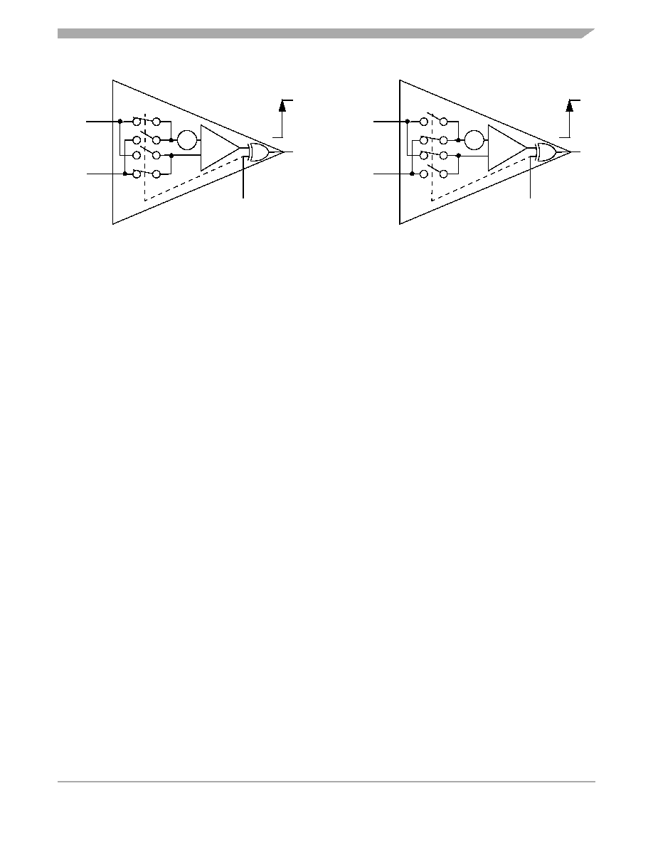
Analog Multiplex Register
MC68HC705JJ7 MC68HC705JP7 Advance Information Data Sheet, Rev. 4.1
Freescale Semiconductor
75
Figure 8-4. INV Bit Action
NOTE
Either comparator may generate an output flag when the inputs are
exchanged due to a change in the state of the INV bit. It is therefore
recommended that the INV bit not be changed while waiting for a
comparator flag. Further, any changes to the state of the INV bit should be
followed by writing a logic 1 to both the CPFR1 and CPFR2 bits to clear any
extraneous CPF1 or CPF2 flags that may have occurred.
VREF
This read/write bit connects the channel select bus to VDD for making a reference voltage
measurement. It cannot be selected if any of the other input sources to the channel select bus are
selected as shown in Table 8-2. This bit is cleared by a reset of the device.
1 = Channel select bus connected to VDD if all MUX1:4 are cleared.
0 = Channel select bus cannot be connected to VDD.
MUX1:4
These are read/write bits that connect the analog subsystem pins to the channel select bus and voltage
comparator 2 for purposes of making a voltage measurement. They can be selected individually or
combined with any of the other input sources to the channel select bus as shown in Table 8-2.
NOTE
voltage generated by the total chip current passing through the package
bond wires and lead frame that are attached to the single VSS pin. This
offset raises the internal VSS reference (AVSS) in the analog subsystem
with respect to the external VSS pin. Turning on the VSS MUX to the channel
select bus connects it to this internal AVSS reference line.
When making A/D conversions, this AVSS offset gets placed on the external
ramping capacitor since the discharge device on the PB0/AN0 pin
discharges the external capacitor to the internal AVSS line. Under these
circumstances, the positive input (+) to comparator 2 will always be higher
than the negative input (–) until the negative input reaches the AVSS offset
voltage plus any offset in comparator 2.
V–
V+
INV = 0
+
COMP
VIO
–
RISE
WHEN
V+ > V–
INV = 1
V+
V–
+
COMP
VIO
–
RISE
WHEN
V+ > V–
相关PDF资料 |
PDF描述 |
|---|---|
| VI-B4L-IX-B1 | CONVERTER MOD DC/DC 28V 75W |
| VI-B4K-IW-B1 | CONVERTER MOD DC/DC 40V 100W |
| VI-B4J-IX-B1 | CONVERTER MOD DC/DC 36V 75W |
| VI-B4J-IW-B1 | CONVERTER MOD DC/DC 36V 100W |
| VI-B43-IX-B1 | CONVERTER MOD DC/DC 24V 75W |
相关代理商/技术参数 |
参数描述 |
|---|---|
| MCHC705JP7CDWE | 功能描述:8位微控制器 -MCU 8B MCU 224 BYTES RAM RoHS:否 制造商:Silicon Labs 核心:8051 处理器系列:C8051F39x 数据总线宽度:8 bit 最大时钟频率:50 MHz 程序存储器大小:16 KB 数据 RAM 大小:1 KB 片上 ADC:Yes 工作电源电压:1.8 V to 3.6 V 工作温度范围:- 40 C to + 105 C 封装 / 箱体:QFN-20 安装风格:SMD/SMT |
| MCHC705KJ1CDWE | 功能描述:8位微控制器 -MCU 8 BIT MCU 64 BYTES RAM RoHS:否 制造商:Silicon Labs 核心:8051 处理器系列:C8051F39x 数据总线宽度:8 bit 最大时钟频率:50 MHz 程序存储器大小:16 KB 数据 RAM 大小:1 KB 片上 ADC:Yes 工作电源电压:1.8 V to 3.6 V 工作温度范围:- 40 C to + 105 C 封装 / 箱体:QFN-20 安装风格:SMD/SMT |
| MCHC705KJ1CDWE | 制造商:Freescale Semiconductor 功能描述:8-Bit Microcontroller IC |
| MCHC705KJ1CPE | 功能描述:IC MCU 8BIT 64 BYTES RAM 16PDIP RoHS:是 类别:集成电路 (IC) >> 嵌入式 - 微控制器, 系列:HC05 标准包装:1 系列:87C 核心处理器:MCS 51 芯体尺寸:8-位 速度:16MHz 连通性:SIO 外围设备:- 输入/输出数:32 程序存储器容量:8KB(8K x 8) 程序存储器类型:OTP EEPROM 大小:- RAM 容量:256 x 8 电压 - 电源 (Vcc/Vdd):4 V ~ 6 V 数据转换器:- 振荡器型:外部 工作温度:0°C ~ 70°C 封装/外壳:44-DIP 包装:管件 其它名称:864285 |
| MCHC711KS2CFNE3 | 功能描述:8位微控制器 -MCU 32K EPROM - SLO MODE RoHS:否 制造商:Silicon Labs 核心:8051 处理器系列:C8051F39x 数据总线宽度:8 bit 最大时钟频率:50 MHz 程序存储器大小:16 KB 数据 RAM 大小:1 KB 片上 ADC:Yes 工作电源电压:1.8 V to 3.6 V 工作温度范围:- 40 C to + 105 C 封装 / 箱体:QFN-20 安装风格:SMD/SMT |
发布紧急采购,3分钟左右您将得到回复。