- 您现在的位置:买卖IC网 > PDF目录10964 > MCHC705JJ7CPE (Freescale Semiconductor)IC MCU 8BIT 224 BYTES RAM 20PDIP PDF资料下载
参数资料
| 型号: | MCHC705JJ7CPE |
| 厂商: | Freescale Semiconductor |
| 文件页数: | 127/164页 |
| 文件大小: | 0K |
| 描述: | IC MCU 8BIT 224 BYTES RAM 20PDIP |
| 标准包装: | 18 |
| 系列: | HC05 |
| 核心处理器: | HC05 |
| 芯体尺寸: | 8-位 |
| 速度: | 2.1MHz |
| 连通性: | SIO |
| 外围设备: | POR,温度传感器,WDT |
| 输入/输出数: | 14 |
| 程序存储器容量: | 6KB(6K x 8) |
| 程序存储器类型: | OTP |
| RAM 容量: | 224 x 8 |
| 电压 - 电源 (Vcc/Vdd): | 2.7 V ~ 5.5 V |
| 数据转换器: | A/D 4x12b |
| 振荡器型: | 内部 |
| 工作温度: | -40°C ~ 85°C |
| 封装/外壳: | 20-DIP(0.300",7.62mm) |
| 包装: | 管件 |
第1页第2页第3页第4页第5页第6页第7页第8页第9页第10页第11页第12页第13页第14页第15页第16页第17页第18页第19页第20页第21页第22页第23页第24页第25页第26页第27页第28页第29页第30页第31页第32页第33页第34页第35页第36页第37页第38页第39页第40页第41页第42页第43页第44页第45页第46页第47页第48页第49页第50页第51页第52页第53页第54页第55页第56页第57页第58页第59页第60页第61页第62页第63页第64页第65页第66页第67页第68页第69页第70页第71页第72页第73页第74页第75页第76页第77页第78页第79页第80页第81页第82页第83页第84页第85页第86页第87页第88页第89页第90页第91页第92页第93页第94页第95页第96页第97页第98页第99页第100页第101页第102页第103页第104页第105页第106页第107页第108页第109页第110页第111页第112页第113页第114页第115页第116页第117页第118页第119页第120页第121页第122页第123页第124页第125页第126页当前第127页第128页第129页第130页第131页第132页第133页第134页第135页第136页第137页第138页第139页第140页第141页第142页第143页第144页第145页第146页第147页第148页第149页第150页第151页第152页第153页第154页第155页第156页第157页第158页第159页第160页第161页第162页第163页第164页
Port B
MC68HC705JJ7 MC68HC705JP7 Advance Information Data Sheet, Rev. 4.1
Freescale Semiconductor
65
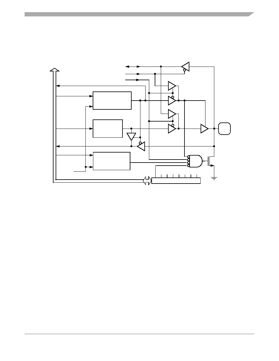
7.3.9 PB7/SCK Logic
The PB7/SCK pin can be used as a simple I/O port pin or be controlled by the SIOP serial interface as
shown in Figure 7-12. The operations of the PB7/SCK pin are summarized in Table 7-3.
Figure 7-12. PB7/SCK Pin I/O Circuit
When using the PB7/SCK pin, these interactions must be noted:
1.
If the SIOP function is required, then the SPE bit in the SCR must be set. This causes the PB7/SCK
pin buffer to be controlled by the MSTR control bit in the SCR. The pulldown device is disabled in
these cases.
a.
If the MSTR bit is set, then the PB7/SCK pin buffer will be enabled and driven by the serial
data clock (SCK) from the SIOP.
b.
If the MSTR bit is clear, then the PB7/SCK pin buffer will be disabled, allowing the PB7/SCK
pin to drive the serial data clock (SCK) into the SIOP.
2.
If the SIOP function is in control of the PB7/SCK pin, the DDRB7 and PB7 data register bits are still
accessible to the CPU and can be altered or read without affecting the SIOP functionality.
However, if the DDRB7 bit is cleared, reading the PB7 data register will return the current state of
the PB7/SCK pin.
3.
If the SIOP function is terminated by clearing the SPE bit in the SCR, then the last conditions stored
in the DDRB7, PDIB7, and PB7 register bits will then control the PB7/SCK pin.
4.
If the PB7/SCK pin is to be a digital input, then both the SPE bit in the SCR and the DDRB7 bit
must be cleared. Depending on the external application, the pulldown device may also be disabled
by setting the PDIB7 pulldown inhibit bit.
DATA DIRECTION
REGISTER B
BIT DDRB7
PORT B DATA
REGISTER
BIT PB7
PULLDOWN
REGISTER B
BIT PDIB7
R
PB7
READ $0005
WRITE $0001
READ $0001
WRITE $0011
PULLDOWN
DEVICE
RESET
IN
T
E
R
N
AL
D
AT
A
BU
S
WRITE $0005
SCK
SERIAL ENABLE (SPE)
CLOCK SOURCE (MSTR)
SERIAL DATA CLOCK (SCK)
SWPDI
MASK OPTION REG. ($1FF1)
相关PDF资料 |
PDF描述 |
|---|---|
| VI-B4L-IX-B1 | CONVERTER MOD DC/DC 28V 75W |
| VI-B4K-IW-B1 | CONVERTER MOD DC/DC 40V 100W |
| VI-B4J-IX-B1 | CONVERTER MOD DC/DC 36V 75W |
| VI-B4J-IW-B1 | CONVERTER MOD DC/DC 36V 100W |
| VI-B43-IX-B1 | CONVERTER MOD DC/DC 24V 75W |
相关代理商/技术参数 |
参数描述 |
|---|---|
| MCHC705JP7CDWE | 功能描述:8位微控制器 -MCU 8B MCU 224 BYTES RAM RoHS:否 制造商:Silicon Labs 核心:8051 处理器系列:C8051F39x 数据总线宽度:8 bit 最大时钟频率:50 MHz 程序存储器大小:16 KB 数据 RAM 大小:1 KB 片上 ADC:Yes 工作电源电压:1.8 V to 3.6 V 工作温度范围:- 40 C to + 105 C 封装 / 箱体:QFN-20 安装风格:SMD/SMT |
| MCHC705KJ1CDWE | 功能描述:8位微控制器 -MCU 8 BIT MCU 64 BYTES RAM RoHS:否 制造商:Silicon Labs 核心:8051 处理器系列:C8051F39x 数据总线宽度:8 bit 最大时钟频率:50 MHz 程序存储器大小:16 KB 数据 RAM 大小:1 KB 片上 ADC:Yes 工作电源电压:1.8 V to 3.6 V 工作温度范围:- 40 C to + 105 C 封装 / 箱体:QFN-20 安装风格:SMD/SMT |
| MCHC705KJ1CDWE | 制造商:Freescale Semiconductor 功能描述:8-Bit Microcontroller IC |
| MCHC705KJ1CPE | 功能描述:IC MCU 8BIT 64 BYTES RAM 16PDIP RoHS:是 类别:集成电路 (IC) >> 嵌入式 - 微控制器, 系列:HC05 标准包装:1 系列:87C 核心处理器:MCS 51 芯体尺寸:8-位 速度:16MHz 连通性:SIO 外围设备:- 输入/输出数:32 程序存储器容量:8KB(8K x 8) 程序存储器类型:OTP EEPROM 大小:- RAM 容量:256 x 8 电压 - 电源 (Vcc/Vdd):4 V ~ 6 V 数据转换器:- 振荡器型:外部 工作温度:0°C ~ 70°C 封装/外壳:44-DIP 包装:管件 其它名称:864285 |
| MCHC711KS2CFNE3 | 功能描述:8位微控制器 -MCU 32K EPROM - SLO MODE RoHS:否 制造商:Silicon Labs 核心:8051 处理器系列:C8051F39x 数据总线宽度:8 bit 最大时钟频率:50 MHz 程序存储器大小:16 KB 数据 RAM 大小:1 KB 片上 ADC:Yes 工作电源电压:1.8 V to 3.6 V 工作温度范围:- 40 C to + 105 C 封装 / 箱体:QFN-20 安装风格:SMD/SMT |
发布紧急采购,3分钟左右您将得到回复。