- 您现在的位置:买卖IC网 > PDF目录10964 > MCHC705JJ7CPE (Freescale Semiconductor)IC MCU 8BIT 224 BYTES RAM 20PDIP PDF资料下载
参数资料
| 型号: | MCHC705JJ7CPE |
| 厂商: | Freescale Semiconductor |
| 文件页数: | 157/164页 |
| 文件大小: | 0K |
| 描述: | IC MCU 8BIT 224 BYTES RAM 20PDIP |
| 标准包装: | 18 |
| 系列: | HC05 |
| 核心处理器: | HC05 |
| 芯体尺寸: | 8-位 |
| 速度: | 2.1MHz |
| 连通性: | SIO |
| 外围设备: | POR,温度传感器,WDT |
| 输入/输出数: | 14 |
| 程序存储器容量: | 6KB(6K x 8) |
| 程序存储器类型: | OTP |
| RAM 容量: | 224 x 8 |
| 电压 - 电源 (Vcc/Vdd): | 2.7 V ~ 5.5 V |
| 数据转换器: | A/D 4x12b |
| 振荡器型: | 内部 |
| 工作温度: | -40°C ~ 85°C |
| 封装/外壳: | 20-DIP(0.300",7.62mm) |
| 包装: | 管件 |
第1页第2页第3页第4页第5页第6页第7页第8页第9页第10页第11页第12页第13页第14页第15页第16页第17页第18页第19页第20页第21页第22页第23页第24页第25页第26页第27页第28页第29页第30页第31页第32页第33页第34页第35页第36页第37页第38页第39页第40页第41页第42页第43页第44页第45页第46页第47页第48页第49页第50页第51页第52页第53页第54页第55页第56页第57页第58页第59页第60页第61页第62页第63页第64页第65页第66页第67页第68页第69页第70页第71页第72页第73页第74页第75页第76页第77页第78页第79页第80页第81页第82页第83页第84页第85页第86页第87页第88页第89页第90页第91页第92页第93页第94页第95页第96页第97页第98页第99页第100页第101页第102页第103页第104页第105页第106页第107页第108页第109页第110页第111页第112页第113页第114页第115页第116页第117页第118页第119页第120页第121页第122页第123页第124页第125页第126页第127页第128页第129页第130页第131页第132页第133页第134页第135页第136页第137页第138页第139页第140页第141页第142页第143页第144页第145页第146页第147页第148页第149页第150页第151页第152页第153页第154页第155页第156页当前第157页第158页第159页第160页第161页第162页第163页第164页
Analog Subsystem
MC68HC705JJ7 MC68HC705JP7 Advance Information Data Sheet, Rev. 4.1
92
Freescale Semiconductor
8.7 Voltage Comparator Features
The two internal comparators can be used as simple voltage comparators if set up as described in
Table 8-8. Both comparators can be active in the wait mode and can directly restart the part by means of
the analog interrupt. Both comparators can also be active in the stop mode, but cannot directly restart the
part. However, the comparators can directly drive PB4 which can then be connected externally to activate
either a port interrupt on the PA0:3 pins or the IRQ/VPP pin.
8.7.1 Voltage Comparator 1
Voltage comparator 1 is always connected to two of the port B I/O pins. These pins should be configured
as inputs and have their software programmable pulldowns disabled. Also, the negative input of voltage
comparator 1 is connected to the PB3/AN3/TCAP and shared with the input capture function of the 16-bit
programmable timer. Therefore, the timer input capture interrupt should be disabled so that changes in
the voltage on the PB3/AN3/TCAP pin do not cause unwanted input capture interrupts.
The output of comparator 1 can be connected to the port logic driving the PB4/AN4/TCMP/CMP1 pin such
that the output of the comparator is ORed with the PB4 data bit and the OLVL bit from the 16-bit timer.
This capability requires that the OPT bit is set in the COPR at location $1FF0 as in Figure 8-12, and the
COE1 bit is set in the ASR at location $001E.
OPT — Optional Features Bit
The OPT bit enables two additional features: direct drive by comparator 1 output to PB4 and voltage
offset capability to sample capacitor in analog subsystem.
1 = Optional features enabled
0 = Optional features disabled
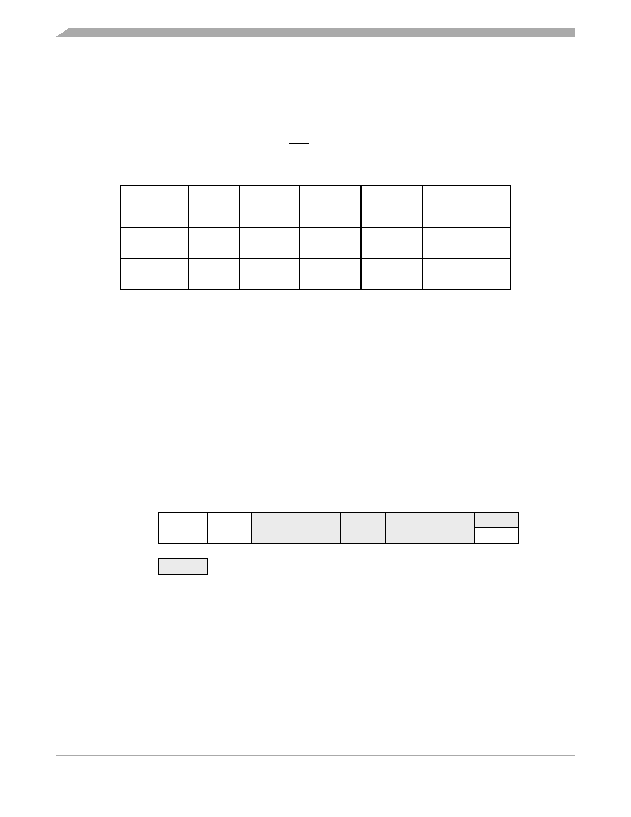
Table 8-8. Voltage Comparator Setup Conditions
Comparator
Current
Source
Enable
Discharge
Device
Disable
Port B Pin
as Inputs
Port B Pin
Pulldowns
Disabled
Prog. Timer Input
Capture
Source
1
Not
affected
Not
affected
DDRB2 = 0
DDRB3 = 0
PDIB2 = 1
PDIB3 = 1
Not
affected
2
ISEN = 0
DDRB0 = 0
DDRB1 = 0
PDIB0 = 1
PDIB1 = 1
ICEN = 0
IEDG = 1
Address:
$1FF0
Bit 7
6
5
4321
Bit 0
Read:
EPMSEC
OPT
Write:
COPC
Reset:
U
UUUUUUU
= Unimplemented
U = Unaffected
Figure 8-12. COP and Security Register (COPR)
相关PDF资料 |
PDF描述 |
|---|---|
| VI-B4L-IX-B1 | CONVERTER MOD DC/DC 28V 75W |
| VI-B4K-IW-B1 | CONVERTER MOD DC/DC 40V 100W |
| VI-B4J-IX-B1 | CONVERTER MOD DC/DC 36V 75W |
| VI-B4J-IW-B1 | CONVERTER MOD DC/DC 36V 100W |
| VI-B43-IX-B1 | CONVERTER MOD DC/DC 24V 75W |
相关代理商/技术参数 |
参数描述 |
|---|---|
| MCHC705JP7CDWE | 功能描述:8位微控制器 -MCU 8B MCU 224 BYTES RAM RoHS:否 制造商:Silicon Labs 核心:8051 处理器系列:C8051F39x 数据总线宽度:8 bit 最大时钟频率:50 MHz 程序存储器大小:16 KB 数据 RAM 大小:1 KB 片上 ADC:Yes 工作电源电压:1.8 V to 3.6 V 工作温度范围:- 40 C to + 105 C 封装 / 箱体:QFN-20 安装风格:SMD/SMT |
| MCHC705KJ1CDWE | 功能描述:8位微控制器 -MCU 8 BIT MCU 64 BYTES RAM RoHS:否 制造商:Silicon Labs 核心:8051 处理器系列:C8051F39x 数据总线宽度:8 bit 最大时钟频率:50 MHz 程序存储器大小:16 KB 数据 RAM 大小:1 KB 片上 ADC:Yes 工作电源电压:1.8 V to 3.6 V 工作温度范围:- 40 C to + 105 C 封装 / 箱体:QFN-20 安装风格:SMD/SMT |
| MCHC705KJ1CDWE | 制造商:Freescale Semiconductor 功能描述:8-Bit Microcontroller IC |
| MCHC705KJ1CPE | 功能描述:IC MCU 8BIT 64 BYTES RAM 16PDIP RoHS:是 类别:集成电路 (IC) >> 嵌入式 - 微控制器, 系列:HC05 标准包装:1 系列:87C 核心处理器:MCS 51 芯体尺寸:8-位 速度:16MHz 连通性:SIO 外围设备:- 输入/输出数:32 程序存储器容量:8KB(8K x 8) 程序存储器类型:OTP EEPROM 大小:- RAM 容量:256 x 8 电压 - 电源 (Vcc/Vdd):4 V ~ 6 V 数据转换器:- 振荡器型:外部 工作温度:0°C ~ 70°C 封装/外壳:44-DIP 包装:管件 其它名称:864285 |
| MCHC711KS2CFNE3 | 功能描述:8位微控制器 -MCU 32K EPROM - SLO MODE RoHS:否 制造商:Silicon Labs 核心:8051 处理器系列:C8051F39x 数据总线宽度:8 bit 最大时钟频率:50 MHz 程序存储器大小:16 KB 数据 RAM 大小:1 KB 片上 ADC:Yes 工作电源电压:1.8 V to 3.6 V 工作温度范围:- 40 C to + 105 C 封装 / 箱体:QFN-20 安装风格:SMD/SMT |
发布紧急采购,3分钟左右您将得到回复。