- 您现在的位置:买卖IC网 > PDF目录10964 > MCHC705JJ7CPE (Freescale Semiconductor)IC MCU 8BIT 224 BYTES RAM 20PDIP PDF资料下载
参数资料
| 型号: | MCHC705JJ7CPE |
| 厂商: | Freescale Semiconductor |
| 文件页数: | 96/164页 |
| 文件大小: | 0K |
| 描述: | IC MCU 8BIT 224 BYTES RAM 20PDIP |
| 标准包装: | 18 |
| 系列: | HC05 |
| 核心处理器: | HC05 |
| 芯体尺寸: | 8-位 |
| 速度: | 2.1MHz |
| 连通性: | SIO |
| 外围设备: | POR,温度传感器,WDT |
| 输入/输出数: | 14 |
| 程序存储器容量: | 6KB(6K x 8) |
| 程序存储器类型: | OTP |
| RAM 容量: | 224 x 8 |
| 电压 - 电源 (Vcc/Vdd): | 2.7 V ~ 5.5 V |
| 数据转换器: | A/D 4x12b |
| 振荡器型: | 内部 |
| 工作温度: | -40°C ~ 85°C |
| 封装/外壳: | 20-DIP(0.300",7.62mm) |
| 包装: | 管件 |
第1页第2页第3页第4页第5页第6页第7页第8页第9页第10页第11页第12页第13页第14页第15页第16页第17页第18页第19页第20页第21页第22页第23页第24页第25页第26页第27页第28页第29页第30页第31页第32页第33页第34页第35页第36页第37页第38页第39页第40页第41页第42页第43页第44页第45页第46页第47页第48页第49页第50页第51页第52页第53页第54页第55页第56页第57页第58页第59页第60页第61页第62页第63页第64页第65页第66页第67页第68页第69页第70页第71页第72页第73页第74页第75页第76页第77页第78页第79页第80页第81页第82页第83页第84页第85页第86页第87页第88页第89页第90页第91页第92页第93页第94页第95页当前第96页第97页第98页第99页第100页第101页第102页第103页第104页第105页第106页第107页第108页第109页第110页第111页第112页第113页第114页第115页第116页第117页第118页第119页第120页第121页第122页第123页第124页第125页第126页第127页第128页第129页第130页第131页第132页第133页第134页第135页第136页第137页第138页第139页第140页第141页第142页第143页第144页第145页第146页第147页第148页第149页第150页第151页第152页第153页第154页第155页第156页第157页第158页第159页第160页第161页第162页第163页第164页
External Interrupts
MC68HC705JJ7 MC68HC705JP7 Advance Information Data Sheet, Rev. 4.1
Freescale Semiconductor
37
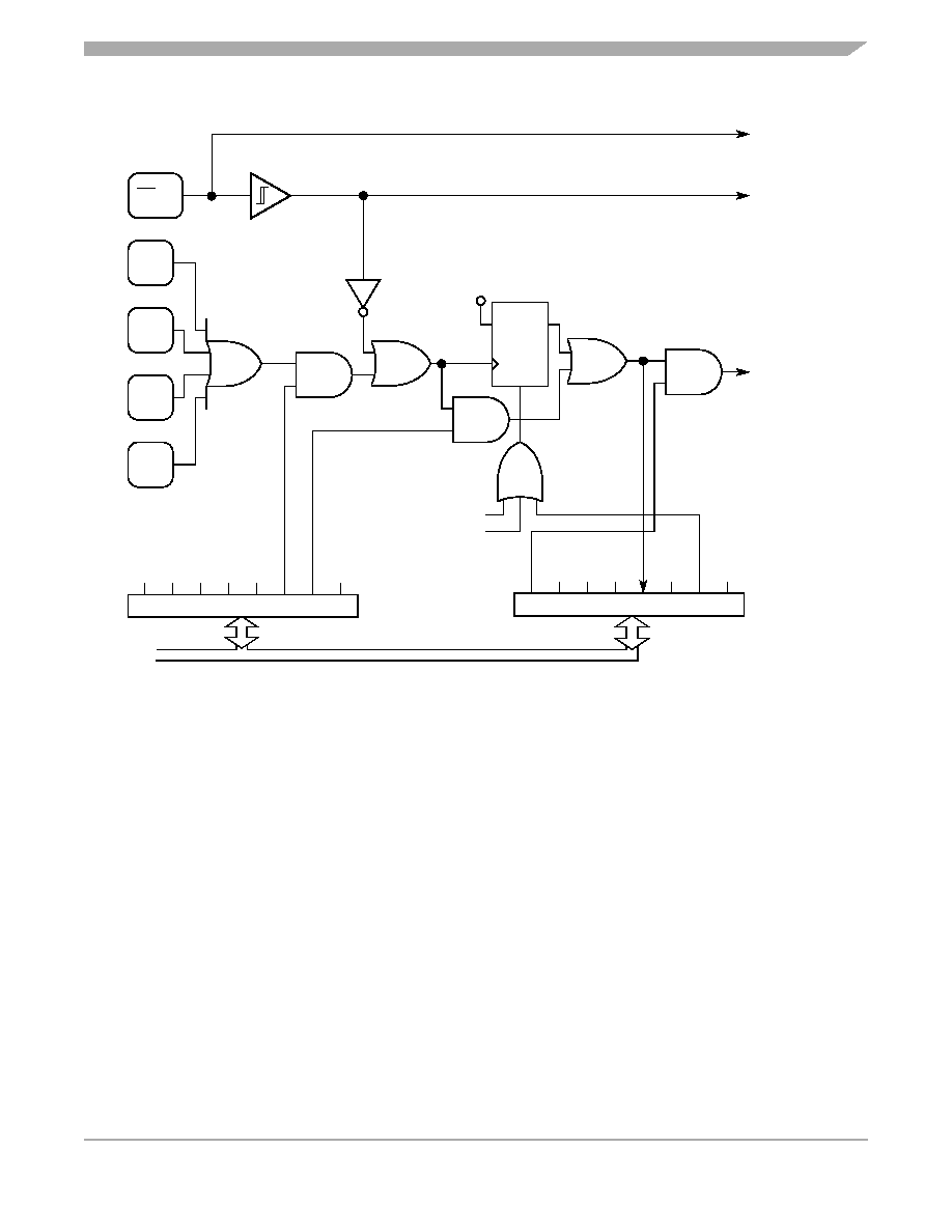
Figure 4-3. External Interrupt Logic
4.5.2 PA0–PA3 Pins
Programming the PIRQ bit in the MOR to a logic 1 enables the PA0–PA3 pins (PA0:3) to serve as
additional external interrupt sources. A rising edge on a PA0:3 pin latches an external interrupt request.
After completing the current instruction, the CPU tests the IRQ latch. If the IRQ latch is set, the CPU then
tests the I bit in the condition code register and the IRQE bit in the ISCR. If the I bit is clear and the IRQE
bit is set, the CPU then begins the interrupt sequence. The CPU clears the IRQ latch while it fetches the
interrupt vector, so that another external interrupt request can be latched during the interrupt service
routine. As soon as the I bit is cleared during the return from interrupt, the CPU can recognize the new
interrupt request.
The PA0:3 pins can be edge-triggered or edge- and level-triggered. External interrupt triggering sensitivity
is selected by the LEVEL bit in the MOR.
With the edge- and level-sensitive trigger MOR option, a rising edge or a high level on a PA0:3 pin latches
an external interrupt request. The edge- and level-sensitive trigger MOR option allows connection to a
PA0:3 pin of multiple wired-OR interrupt sources. As long as any source is holding the pin high, an
external interrupt request is present, and the CPU continues to execute the interrupt service routine.
PA3
PA2
PA1
PA0
IRQ
LATCH
VDD
RST
IRQ VECTOR FETCH
IRQ STATUS/CONTROL REGISTER ($000D)
EXTERNAL
INTERRUPT
REQUEST
IR
QE
IR
QF
IR
QR
INTERNAL DATA BUS
TO BIH & BIL
INSTRUCTION
PROCESSING
R
PIRQ
LEVEL
VPP TO
USER EPROM
AND PEPROM
MASK OPTION REGISTER ($1FF1)
IRQ/VPP
相关PDF资料 |
PDF描述 |
|---|---|
| VI-B4L-IX-B1 | CONVERTER MOD DC/DC 28V 75W |
| VI-B4K-IW-B1 | CONVERTER MOD DC/DC 40V 100W |
| VI-B4J-IX-B1 | CONVERTER MOD DC/DC 36V 75W |
| VI-B4J-IW-B1 | CONVERTER MOD DC/DC 36V 100W |
| VI-B43-IX-B1 | CONVERTER MOD DC/DC 24V 75W |
相关代理商/技术参数 |
参数描述 |
|---|---|
| MCHC705JP7CDWE | 功能描述:8位微控制器 -MCU 8B MCU 224 BYTES RAM RoHS:否 制造商:Silicon Labs 核心:8051 处理器系列:C8051F39x 数据总线宽度:8 bit 最大时钟频率:50 MHz 程序存储器大小:16 KB 数据 RAM 大小:1 KB 片上 ADC:Yes 工作电源电压:1.8 V to 3.6 V 工作温度范围:- 40 C to + 105 C 封装 / 箱体:QFN-20 安装风格:SMD/SMT |
| MCHC705KJ1CDWE | 功能描述:8位微控制器 -MCU 8 BIT MCU 64 BYTES RAM RoHS:否 制造商:Silicon Labs 核心:8051 处理器系列:C8051F39x 数据总线宽度:8 bit 最大时钟频率:50 MHz 程序存储器大小:16 KB 数据 RAM 大小:1 KB 片上 ADC:Yes 工作电源电压:1.8 V to 3.6 V 工作温度范围:- 40 C to + 105 C 封装 / 箱体:QFN-20 安装风格:SMD/SMT |
| MCHC705KJ1CDWE | 制造商:Freescale Semiconductor 功能描述:8-Bit Microcontroller IC |
| MCHC705KJ1CPE | 功能描述:IC MCU 8BIT 64 BYTES RAM 16PDIP RoHS:是 类别:集成电路 (IC) >> 嵌入式 - 微控制器, 系列:HC05 标准包装:1 系列:87C 核心处理器:MCS 51 芯体尺寸:8-位 速度:16MHz 连通性:SIO 外围设备:- 输入/输出数:32 程序存储器容量:8KB(8K x 8) 程序存储器类型:OTP EEPROM 大小:- RAM 容量:256 x 8 电压 - 电源 (Vcc/Vdd):4 V ~ 6 V 数据转换器:- 振荡器型:外部 工作温度:0°C ~ 70°C 封装/外壳:44-DIP 包装:管件 其它名称:864285 |
| MCHC711KS2CFNE3 | 功能描述:8位微控制器 -MCU 32K EPROM - SLO MODE RoHS:否 制造商:Silicon Labs 核心:8051 处理器系列:C8051F39x 数据总线宽度:8 bit 最大时钟频率:50 MHz 程序存储器大小:16 KB 数据 RAM 大小:1 KB 片上 ADC:Yes 工作电源电压:1.8 V to 3.6 V 工作温度范围:- 40 C to + 105 C 封装 / 箱体:QFN-20 安装风格:SMD/SMT |
发布紧急采购,3分钟左右您将得到回复。