- 您现在的位置:买卖IC网 > PDF目录45332 > MKI41T56S00TR (STMICROELECTRONICS) 0 TIMER(S), REAL TIME CLOCK, PDSO8 PDF资料下载
参数资料
| 型号: | MKI41T56S00TR |
| 厂商: | STMICROELECTRONICS |
| 元件分类: | 时钟/数据恢复及定时提取 |
| 英文描述: | 0 TIMER(S), REAL TIME CLOCK, PDSO8 |
| 封装: | 0.150 INCH, PLASTIC, SOP-8 |
| 文件页数: | 14/16页 |
| 文件大小: | 105K |
| 代理商: | MKI41T56S00TR |
7/16
MK41T56, MKI41T56
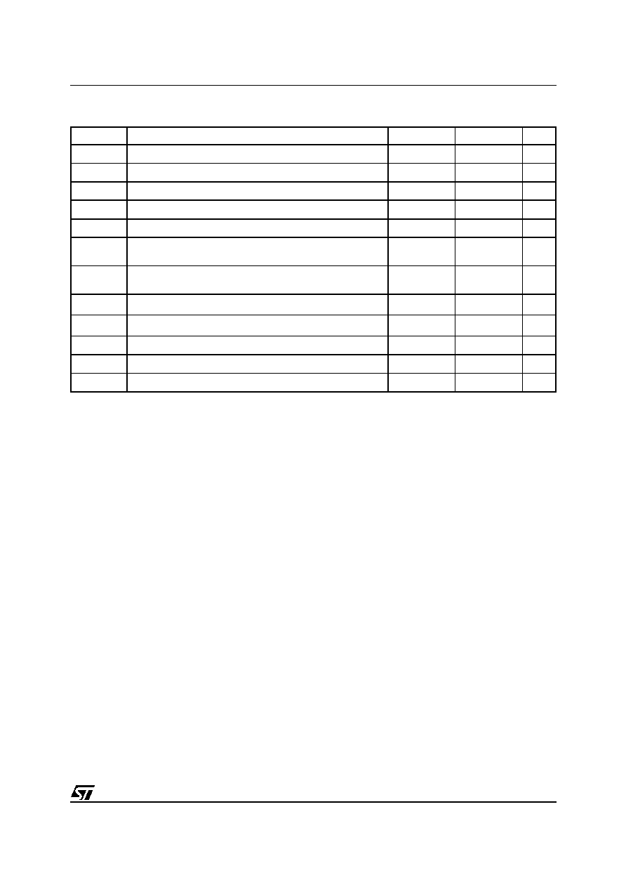
Table 10. AC Characteristics
(TA = 0 to 70 °C or –40 to 85°C; VCC = 4.5V to 5.5V)
Note: 1. Transmitter must internally provide a hold time to bridge the undefined region (300ns max.) of the falling edge of SCL.
Symbol
Parameter
Min
Max
Unit
fSCL
SCL Clock Frequency
0
100
kHz
tLOW
Clock Low Period
4.7
s
tHIGH
Clock High Period
4
s
tR
SDA and SCL Rise Time
1
s
tF
SDA and SCL Fall Time
300
ns
tHD:STA
START Condition Hold Time
(after this period the first clock pulse is generated)
4s
tSU:STA
START Condition Setup Time
(only relevant for a repeated start condition)
4.7
s
tSU:DAT
(1)
Data Setup Time
250
ns
tHD:DAT
Data Hold Time
0
s
tSU:STO
STOP Condition Setup Time
4.7
s
tBUF
Time the bus must be free before a new transmission can start
4.7
s
tI
Noise suppression time constant at SCL and SDA input
0.25
1
s
of data bytes transferred between the start and
stop conditions is not limited. The information is
transmitted byte-wide and each receiver acknowl-
edges with a ninth bit.
By definition, a device that gives out a message is
called "transmitter", the receiving device that gets
the message is called "receiver". The device that
controls the message is called "master". The de-
vices that are controlled by the master are called
"slaves".
Acknowledge. Each byte of eight bits is followed
by one acknowledge bit. This acknowledge bit is a
low level put on the bus by the receiver, whereas
the master generates an extra acknowledge relat-
ed clock pulse.
A slave receiver which is addressed is obliged to
generate an acknowledge after the reception of
each byte. Also, a master receiver must generate
an acknowledge after the reception of each byte
that has been clocked out of the slave transmitter.
The device that acknowledges has to pull down
the SDA line during the acknowledge clock pulse
in such a way that the SDA line is a stable Low dur-
ing the High period of the acknowledge related
clock pulse. Of course, setup and hold times must
be taken into account. A master receiver must sig-
nal an end-of-data to the slave transmitter by not
generating an acknowledge on the last byte that
has been clocked out of the slave. In this case, the
transmitter must leave the data line High to enable
the master to generate the STOP condition.
相关PDF资料 |
PDF描述 |
|---|---|
| ML2035IP | 1-BIT, DSP-NUM CONTROLLED OSCILLATOR, PDIP8 |
| ML54053 | IDE COMPATIBLE, FLASH MEMORY DRIVE CONTROLLER, PQFP120 |
| ML610Q346J-NNNTB | 8-BIT, FLASH, 4.2 MHz, RISC MICROCONTROLLER, PQFP64 |
| ML610Q409-NNNTBZ03A | RISC MICROCONTROLLER, PQFP100 |
| ML610Q408-NNNTBZ03A | RISC MICROCONTROLLER, PQFP100 |
相关代理商/技术参数 |
参数描述 |
|---|---|
| MKI50-06A7 | 功能描述:IGBT 模块 50 Amps 600V RoHS:否 制造商:Infineon Technologies 产品:IGBT Silicon Modules 配置:Dual 集电极—发射极最大电压 VCEO:600 V 集电极—射极饱和电压:1.95 V 在25 C的连续集电极电流:230 A 栅极—射极漏泄电流:400 nA 功率耗散:445 W 最大工作温度:+ 125 C 封装 / 箱体:34MM 封装: |
| MKI50-06A7T | 功能描述:分立半导体模块 50 Amps 600V RoHS:否 制造商:Infineon Technologies 产品:Thyristor Power Modules 类型:Phase Controls 安装风格:Screw 封装 / 箱体:DT61 封装: |
| MKI50-12E7 | 功能描述:分立半导体模块 IGBT (NPT3) 1200V 50A RoHS:否 制造商:Infineon Technologies 产品:Thyristor Power Modules 类型:Phase Controls 安装风格:Screw 封装 / 箱体:DT61 封装: |
| MKI50-12F7 | 功能描述:IGBT 模块 50 Amps 1200V RoHS:否 制造商:Infineon Technologies 产品:IGBT Silicon Modules 配置:Dual 集电极—发射极最大电压 VCEO:600 V 集电极—射极饱和电压:1.95 V 在25 C的连续集电极电流:230 A 栅极—射极漏泄电流:400 nA 功率耗散:445 W 最大工作温度:+ 125 C 封装 / 箱体:34MM 封装: |
| MKI65-06A7T | 功能描述:分立半导体模块 65 Amps 600V RoHS:否 制造商:Infineon Technologies 产品:Thyristor Power Modules 类型:Phase Controls 安装风格:Screw 封装 / 箱体:DT61 封装: |
发布紧急采购,3分钟左右您将得到回复。