- 您现在的位置:买卖IC网 > PDF目录2099 > MPC9600AE (IDT, Integrated Device Technology Inc)IC PLL CLK DRIVER LV 48-LQFP PDF资料下载
参数资料
| 型号: | MPC9600AE |
| 厂商: | IDT, Integrated Device Technology Inc |
| 文件页数: | 2/15页 |
| 文件大小: | 0K |
| 描述: | IC PLL CLK DRIVER LV 48-LQFP |
| 标准包装: | 250 |
| 类型: | PLL 时钟驱动器 |
| PLL: | 带旁路 |
| 输入: | LVCMOS,LVPECL |
| 输出: | LVCMOS |
| 电路数: | 1 |
| 比率 - 输入:输出: | 2:21 |
| 差分 - 输入:输出: | 是/无 |
| 频率 - 最大: | 200MHz |
| 除法器/乘法器: | 是/是 |
| 电源电压: | 2.375 V ~ 3.465 V |
| 工作温度: | -40°C ~ 85°C |
| 安装类型: | 表面贴装 |
| 封装/外壳: | 48-LQFP |
| 供应商设备封装: | 48-TQFP(7x7) |
| 包装: | 托盘 |
MPC9600 REVISION 6 JANUARY 7, 2013
10
2013 Integrated Device Technology, Inc.
MPC9600 Data Sheet
LOW VOLTAGE, 2.5V AND 3.3V LVCMOS PLL CLOCK DRIVER
Due to the statistical nature of I/O jitter a RMS value (1
) is
specified. I/O jitter numbers for other confidence factors (CF) can
be derived from Table 11.
The feedback trace delay is determined by the board layout
and can be used to fine-tune the effective delay through each
device. In the following example calculation a
I/O jitter confidence factor of 99.7% (
3) is assumed, resulting
in a worst case timing uncertainty from input to any output of –
261 ps to 341 ps relative to CCLK (VCC = 3.3 V and fVCO = 200
MHz):
tSK(PP) = [–60 ps...140 ps] + [–150 ps...150 ps] +
[(17 ps @ –3)...(17 ps @ 3)] + tPD, LINE(FB)
tSK(PP) = [–261 ps...341 ps] + tPD, LINE(FB)
Above equation uses the maximum I/O jitter number shown in
the AC characteristic table for VCC = 3.3 V (17 ps RMS). I/O jitter
is frequency dependant with a maximum at the lowest VCO
frequency (200 MHz for the MPC9600). Applications using a
higher VCO frequency exhibit less I/O jitter than the AC
characteristic limit. The I/O jitter characteristics in Figure 7 can be
used to derive a smaller
I/O jitter number at the specific VCO frequency, resulting in tighter
timing limits in zero-delay mode and for part-to-part skew tSK(PP).
Figure 7. I/O Jitter versus VCO Frequency for
VCC = 2.5 V and VCC = 3.3 V
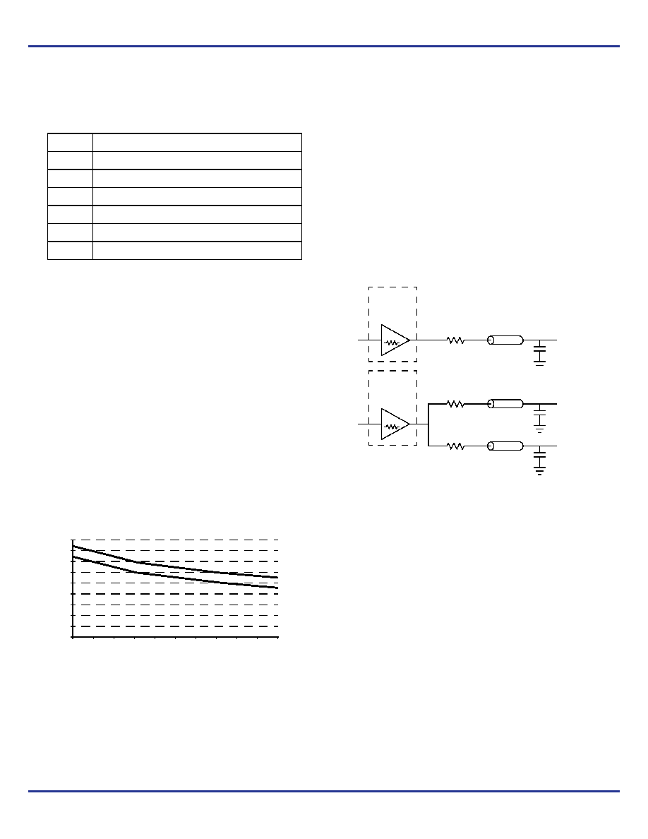
Driving Transmission Lines
The MPC9600 clock driver was designed to drive high speed
signals in a terminated transmission line environment. To provide
the optimum flexibility to the user the output drivers were designed
to exhibit the lowest impedance possible. With an output
impedance of less than 20
the drivers can drive either parallel
or series terminated transmission lines. For more information on
transmission lines the reader is referred to Freescale
Semiconductor application note AN1091. In most high
performance clock networks point-to-point distribution of signals
is the method of choice. In a point-to-point scheme either series
terminated or parallel terminated transmission lines can be used.
The parallel technique terminates the signal at the end of the line
with a 50
resistance to VCC 2.
This technique draws a fairly high level of DC current and thus
only a single terminated line can be driven by each output of the
MPC9600 clock driver. For the series terminated case however
there is no DC current draw, thus the outputs can drive multiple
series terminated lines. Figure 8 illustrates an output driving a
single series terminated line versus two series terminated lines in
parallel. When taken to its extreme the fanout of the MPC9600
clock driver is effectively doubled due to its capability to drive
multiple lines.
Figure 8. Single versus Dual Transmission Lines
The waveform plots in Figure 9 shows the simulation results of
an output driving a single line versus two lines. In both cases the
drive capability of the MPC9600 output buffer is more than
sufficient to drive 50
transmission lines on the incident edge.
Note from the delay measurements in the simulations a delta of
only 43 ps exists between the two differently loaded outputs. This
suggests that the dual line driving need not be used exclusively to
maintain the tight output-to-output skew of the MPC9600. The
output waveform in Figure 9 shows a step in the waveform, this
step is caused by the impedance mismatch seen looking into the
driver. The parallel combination of the 36
series resistor plus the
output impedance does not match the parallel combination of the
line impedances. The voltage wave launched down the two lines
will equal:
VL =VS (Z0 (RS + R0 + Z0))
Z0 =50 || 50
RS =36 || 36
R0 =14
VL = 3.0 (25 (18 + 17 + 25)
=1.31 V
Table 11. Confidence Factor CF
CF
Probability of Clock Edge Within the Distribution
1
0.68268948
2
0.95449988
3
0.99730007
4
0.99993663
5
0.99999943
6
0.99999999
18
16
14
12
10
8
6
4
2
0
200 220 240 260 280 300 320 340 360 380 400
VCO FREQUENCY (MHz)
VCC = 3.3 V
VCC = 2.5 V
Maximum I/O Jitter versus Frequency
tji
t(
)[p
s]
rms
14
IN
MPC9600
Output
Buffer
RS = 36
ZO = 50
OutA
14
IN
MPC9600
Output
Buffer
RS = 36
ZO = 50
OutB0
RS = 36
ZO = 50
OutB1
相关PDF资料 |
PDF描述 |
|---|---|
| MPC961CAC | IC BUFFER ZD 1:18 PLL 32-LQFP |
| MPC961PAC | IC BUFFER ZD 1:18 PLL 32-LQFP |
| MPC9653AAC | IC PLL CLK GEN 1:8 3.3V 32-LQFP |
| MPC9658AC | IC PLL CLK GEN 1:10 3.3V 32-LQFP |
| MPC9772FA | IC PLL CLK GEN 1:12 3.3V 52-LQFP |
相关代理商/技术参数 |
参数描述 |
|---|---|
| MPC9600AER2 | 功能描述:时钟缓冲器 RoHS:否 制造商:Texas Instruments 输出端数量:5 最大输入频率:40 MHz 传播延迟(最大值): 电源电压-最大:3.45 V 电源电压-最小:2.375 V 最大功率耗散: 最大工作温度:+ 85 C 最小工作温度:- 40 C 封装 / 箱体:LLP-24 封装:Reel |
| MPC9600FA | 功能描述:IC CLOCK DRVR PLL LV 1:21 48LQFP RoHS:否 类别:集成电路 (IC) >> 时钟/计时 - 时钟发生器,PLL,频率合成器 系列:- 标准包装:39 系列:- 类型:* PLL:带旁路 输入:时钟 输出:时钟 电路数:1 比率 - 输入:输出:1:10 差分 - 输入:输出:是/是 频率 - 最大:170MHz 除法器/乘法器:无/无 电源电压:2.375 V ~ 3.465 V 工作温度:0°C ~ 70°C 安装类型:* 封装/外壳:* 供应商设备封装:* 包装:* |
| MPC9608 | 制造商:MOTOROLA 制造商全称:Motorola, Inc 功能描述:1:10 LVCMOS Zero Delay Clock Buffer |
| MPC9608AC | 功能描述:时钟缓冲器 RoHS:否 制造商:Texas Instruments 输出端数量:5 最大输入频率:40 MHz 传播延迟(最大值): 电源电压-最大:3.45 V 电源电压-最小:2.375 V 最大功率耗散: 最大工作温度:+ 85 C 最小工作温度:- 40 C 封装 / 箱体:LLP-24 封装:Reel |
| MPC9608ACR2 | 功能描述:时钟缓冲器 RoHS:否 制造商:Texas Instruments 输出端数量:5 最大输入频率:40 MHz 传播延迟(最大值): 电源电压-最大:3.45 V 电源电压-最小:2.375 V 最大功率耗散: 最大工作温度:+ 85 C 最小工作温度:- 40 C 封装 / 箱体:LLP-24 封装:Reel |
发布紧急采购,3分钟左右您将得到回复。