- 您现在的位置:买卖IC网 > PDF目录385639 > MT28F200B5 (Micron Technology, Inc.) FLASH MEMORY PDF资料下载
参数资料
| 型号: | MT28F200B5 |
| 厂商: | Micron Technology, Inc. |
| 英文描述: | FLASH MEMORY |
| 中文描述: | 闪存 |
| 文件页数: | 14/31页 |
| 文件大小: | 558K |
| 代理商: | MT28F200B5 |
第1页第2页第3页第4页第5页第6页第7页第8页第9页第10页第11页第12页第13页当前第14页第15页第16页第17页第18页第19页第20页第21页第22页第23页第24页第25页第26页第27页第28页第29页第30页第31页
14
2Mb Smart 3 Boot Block Flash Memory
F48.p65 – Rev. 1/00
Micron Technology, Inc., reserves the right to change products or specifications without notice.
2000, Micron Technology, Inc.
2Mb
SMART 3 BOOT BLOCK FLASH MEMORY
WRITE/ERASE CY CLE ENDURANCE
The MT28F002B3 and MT28F200B3 are designed
and fabricated to meet advanced firmware storage re-
quirements. To ensure this level of reliability, V
PP
must
be at 3.3V
±
0.3V or 5V
±
10% during write or erase
cycles. For SmartVoltage-compatible production pro-
gramming, 12V V
PP
is supported for a maximum of 100
cycles and may be connected for up to 100 cumulative
hours. Operation outside these limits may reduce the
number of write and erase cycles that can be performed
on the device.
POWER USAGE
The MT28F002B3 and MT28F200B3 offer several
power-saving features that may be utilized in the array
read mode to conserve power. Deep power-down mode
is enabled by bringing RP# LOW. Current draw (I
CC
) in
this mode is a maximum of 8
μ
A at 3.3V V
CC
. With CE#
LOW, the device will enter idle current mode when it
is not being accessed. In this mode, the maximum I
CC
current is 2mA at 3.3V V
CC
. When CE# is HIGH, the
device will enter standby mode. In this mode, maxi-
mum I
CC
current is 100
μ
A at 3.3V V
CC
. If CE# is brought
HIGH during a WRITE or ERASE, the ISM will continue
to operate, and the device will consume the respective
active power until the WRITE or ERASE is
completed.
POWER-UP
The likelihood of unwanted WRITE or ERASE opera-
tions is minimized since two consecutive cycles are
required to execute either operation. However, to reset
the ISM and to provide additional protection while V
CC
is ramping, one of the following conditions must be
met:
RP# must be held LOW until V
CC
is at valid
functional level;
or
CE# or WE# may be held HIGH and
RP# must be toggled from V
CC
-GND-V
CC
.
After a power-up or RESET, the status register is reset,
and the device will enter the array read mode.
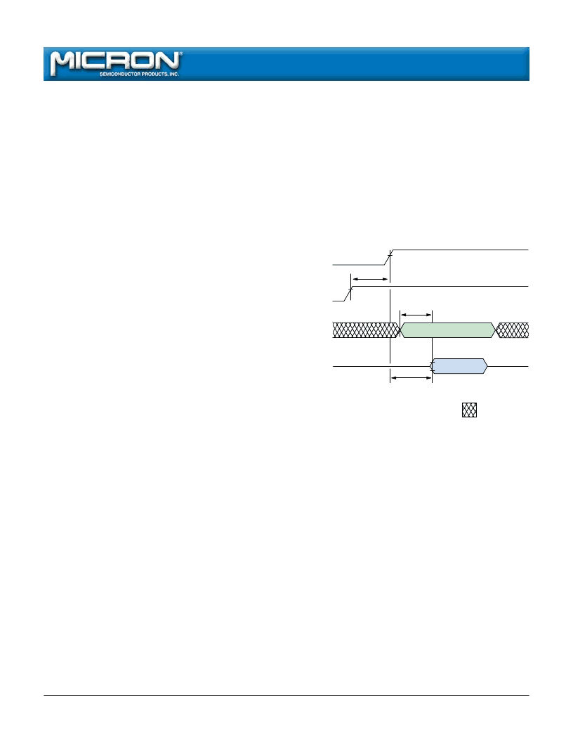
Figure 2
Pow er-Up/Reset Timing Diagram
VALID
VALID
V
CC
(3.3V)
Data
Address
t
Note 1
RP#
RWH
tAA
NOTE:
1. V
CC
must be within the valid operating range before RP#
goes HIGH.
UNDEFINED
相关PDF资料 |
PDF描述 |
|---|---|
| MT28F320A18 | FLASH MEMORY |
| MT2D18 | 1 Meg x 8 DRAM Module(5V,1M x 8 动态RAM模块) |
| MT46V16M4 | 4 Meg x 4 x 4 banks DDR SDRAM(4 M x 4 x 4组,双数据速率同步动态RAM) |
| MT46V4M16 | 1 Meg x 16 x 4 banks DDR SDRAM(1M x 16 x 4组,双数据速率同步动态RAM) |
| MT46V8M8 | 2 Meg x 8 x 4 banks DDR SDRAM(2 M x 8 x 4组,双数据速率同步动态RAM) |
相关代理商/技术参数 |
参数描述 |
|---|---|
| MT28F200B5SG-6 B | 制造商:Micron Technology Inc 功能描述:NOR Flash Parallel 5V 2Mbit 256K/128K x 8bit/16bit 60ns 44-Pin SOP Tray |
| MT28F200B5SG-6 T | 制造商:Micron Technology Inc 功能描述:NOR Flash Parallel 5V 2Mbit 256K/128K x 8bit/16bit 60ns 44-Pin SOP Tray |
| MT28F200B5SG-8 B TR | 制造商:Micron Technology Inc 功能描述:Flash Mem Parallel 5V 2M-Bit 256K x 8/128K x 16 80ns 44-Pin SOP T/R |
| MT28F320A18 | 制造商:MICRON 制造商全称:Micron Technology 功能描述:FLASH MEMORY |
| MT28F320J3 | 制造商:MICRON 制造商全称:Micron Technology 功能描述:Q-FLASHTM MEMORY |
发布紧急采购,3分钟左右您将得到回复。