- 您现在的位置:买卖IC网 > PDF目录385639 > MT46V2M32LG (Micron Technology, Inc.) DOUBLE DATA RATE DDR SDRAM PDF资料下载
参数资料
| 型号: | MT46V2M32LG |
| 厂商: | Micron Technology, Inc. |
| 英文描述: | DOUBLE DATA RATE DDR SDRAM |
| 中文描述: | 双倍数据速率的DDR SDRAM内存 |
| 文件页数: | 9/65页 |
| 文件大小: | 2360K |
| 代理商: | MT46V2M32LG |
第1页第2页第3页第4页第5页第6页第7页第8页当前第9页第10页第11页第12页第13页第14页第15页第16页第17页第18页第19页第20页第21页第22页第23页第24页第25页第26页第27页第28页第29页第30页第31页第32页第33页第34页第35页第36页第37页第38页第39页第40页第41页第42页第43页第44页第45页第46页第47页第48页第49页第50页第51页第52页第53页第54页第55页第56页第57页第58页第59页第60页第61页第62页第63页第64页第65页
9
64Mb: x32 DDR SDRAM
2M32DDR-07.p65
–
Rev. 12/01
Micron Technology, Inc., reserves the right to change products or specifications without notice.
2001, Micron Technology, Inc.
64Mb: x32
DDR SDRAM
Table 2
CAS Latency
Operating Mode
The normal operating mode is selected by issuing a
MODE REGISTER SET command with bits A7-A10 each
set to zero, and bits A0-A6 set to the desired values. A
DLL reset is initiated by issuing a MODE REGISTER
SET command with bits A7, A9 - A10 each set to zero, bit
A8 set to one, and bits A0-A6 set to the desired values.
Although not required by the Micron device, JEDEC
specifications recommend when a LOAD MODE REG-
ISTER command is issued to reset the DLL, it should
always be followed by a LOAD MODE REGISTER com-
mand to select normal operating mode.
All other combinations of values for A7-A10 are re-
served for future use and/or test modes. Test modes
and reserved states should not be used because un-
known operation or incompatibility with future ver-
sions may result.
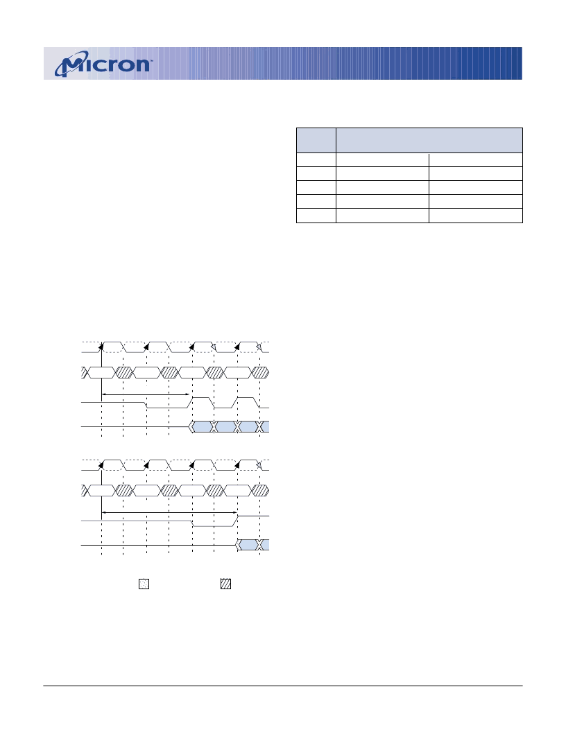
Figure 2
CAS Latency
CK
CK#
COMMAND
DQ
DQS
CL = 2
READ
NOP
NOP
NOP
READ
NOP
NOP
NOP
Burst Length = 4 in the cases shown
Shown with nominal tAC and nominal tDSDQ
CK
CK#
COMMAND
DQ
DQS
CL = 3
T0
T1
T2
T2n
T3
T3n
T0
T1
T2
T3
T3n
DON
’
T CARE
TRANSITIONING DATA
ALLOWABLE OPERATING
FREQUENCY (MHz)
CL = 2
83
≤
f
≤
125
83
≤
f
≤
100
83
≤
f
≤
100
83
≤
f
≤
100
SPEED
-5
-55
-6
-65
CL = 3
83
≤
f
≤
200
83
≤
f
≤
183
83
≤
f
≤
166
83
≤
f
≤
150
Burst Type
Accesses within a given burst may be programmed
to be either sequential or interleaved; this is referred to
as the burst type and is selected via bit M3.
The ordering of accesses within a burst is deter-
mined by the burst length, the burst type and the start-
ing column address, as shown in Table 1.
Read Latency
The READ latency is the delay, in clock cycles, be-
tween the registration of a READ command and the
availability of the first bit of output data. The latency
can be set to 2 or 3 clocks, as shown in Figure 2.
If a READ command is registered at clock edge
n
,
and the latency is
m
clocks, the data will be available
nominally coincident with clock edge
n + m
. Table 2
indicates the operating frequencies at which each CAS
latency setting can be used.
Reserved states should not be used as unknown
operation or incompatibility with future versions may
result.
相关PDF资料 |
PDF描述 |
|---|---|
| MT46V2M32V1 | DOUBLE DATA RATE DDR SDRAM |
| MT46V32M4-1 | DOUBLE DATA RATE DDR SDRAM |
| MT46V32M4TG-75 | DOUBLE DATA RATE DDR SDRAM |
| MT46V32M4TG-75L | DOUBLE DATA RATE DDR SDRAM |
| MT46V32M4TG-75Z | DOUBLE DATA RATE DDR SDRAM |
相关代理商/技术参数 |
参数描述 |
|---|---|
| MT46V2M32V1 | 制造商:MICRON 制造商全称:Micron Technology 功能描述:DOUBLE DATA RATE DDR SDRAM |
| MT46V32M16 | 制造商:Micron Technology Inc 功能描述:32MX16 DDR SDRAM PLASTIC IND TEMP BGA 2.6V DDR - Trays |
| MT46V32M16-5B | 制造商:Micron Technology Inc 功能描述: |
发布紧急采购,3分钟左右您将得到回复。