- 您现在的位置:买卖IC网 > PDF目录20308 > NCP1608BDR2G (ON Semiconductor)IC PFC CTLR/PRECONVERTER 8-SOIC PDF资料下载
参数资料
| 型号: | NCP1608BDR2G |
| 厂商: | ON Semiconductor |
| 文件页数: | 12/24页 |
| 文件大小: | 0K |
| 描述: | IC PFC CTLR/PRECONVERTER 8-SOIC |
| 标准包装: | 1 |
| 模式: | 临界传导(CRM) |
| 电流 - 启动: | 24µA |
| 电源电压: | 10.2 V ~ 20 V |
| 工作温度: | -40°C ~ 125°C |
| 安装类型: | 表面贴装 |
| 封装/外壳: | 8-SOIC(0.154",3.90mm 宽) |
| 供应商设备封装: | 8-SOICN |
| 包装: | 标准包装 |
| 其它名称: | NCP1608BDR2GOSDKR |
�� �
�
�NCP1608�
�When� the� switch� is� closed,� the� inductor� current� increases�
�linearly� to� the� peak� value.� When� the� switch� opens,� the�
�inductor� current� linearly� decreases� to� zero.� When� the�
�inductor� current� decreases� to� zero,� the� drain� voltage� of� the�
�switch� (V� drain� )� is� floating� and� begins� to� decrease.� If� the� next�
�switching� cycle� does� not� begin,� then� V� drain� rings� towards�
�V� in� .� A� derivation� of� equations� found� in� AND8123� leads� to�
�the� result� that� high� power� factor� in� CrM� operation� is�
�V� in(peak)�
�I� L(peak)�
�I� in(peak)�
�V� in� (t)�
�I� L� (t)�
�I� in� (t)�
�ton� +� (eq.� 1)�
�achieved� when� the� on� time� (t� on� )� of� the� switch� is� constant�
�during� an� ac� cycle� and� is� calculated� using� Equation� 1.�
�2� @� P� out� @� L�
�h� @� Vac� 2�
�MOSFET�
�ON�
�OFF�
�Where� P� out� is� the� output� power,� L� is� the� inductor� value,� h�
�is� the� efficiency,� and� Vac� is� the� rms� input� voltage.�
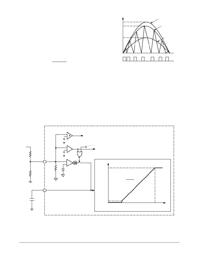
�A� description� of� the� switching� over� an� ac� line� cycle� is�
�illustrated� in� Figure� 28.� The� on� time� is� constant,� but� the� off�
�time� varies� and� is� dependent� on� the� instantaneous� line�
�voltage.� The� constant� on� time� causes� the� peak� inductor�
�current� (I� L(peak)� )� to� scale� with� the� ac� line� voltage.� The�
�NCP1608� represents� an� ideal� method� to� implement� a�
�constant� on� time� CrM� control� in� a� cost� ?� effective� and� robust�
�solution� by� incorporating� an� accurate� regulation� circuit,� a�
�low� current� consumption� startup� circuit,� and� advanced�
�protection� features.�
�Figure� 28.� Inductor� Waveform� During� CrM� Operation�
�Error� Amplifier� Regulation�
�The� NCP1608� regulates� the� boost� output� voltage� using�
�an� internal� error� amplifier� (EA).� The� negative� terminal� of�
�the� EA� is� pinned� out� to� FB,� the� positive� terminal� is�
�connected� to� a� 2.5� V� ±� 1.6%� reference� (V� REF� ),� and� the� EA�
�output� is� pinned� out� to� Control� (Figure� 29).�
�A� feature� of� using� a� transconductance� error� amplifier� is�
�that� the� FB� pin� voltage� is� only� determined� by� the� resistor�
�divider� network� connected� to� the� output� voltage,� not� the�
�operation� of� the� amplifier.� This� enables� the� FB� pin� to� be�
�used� for� sensing� overvoltage� or� undervoltage� conditions�
�independently� of� the� error� amplifier.�
�+� OVP�
�?�
�OVP� Fault�
�V� out�
�V� OVP�
�?� UVP�
�+�
�POK�
�UVP� Fault�
�R� out1�
�R� out2�
�FB�
�R� FB�
�V� UVP�
�EA�
�?�
�+�
�gm�
�V� REF�
�(Enable� EA)�
�t� on(MAX)�
�PWM� BLOCK�
�Slope� +�
�Ct�
�I� charge�
�Control�
�C� COMP�
�V� Control�
�t� on�
�t� PWM�
�Ct� (offset)�
�V� EAH�
�V� Control�
�Figure� 29.� Error� Amplifier� and� On� Time� Regulation� Circuits�
�http://onsemi.com�
�12�
�相关PDF资料 |
PDF描述 |
|---|---|
| PSA15R-060PV | ADAPTER WALL R-SERIES 15W 6V |
| PSA15R-050PV | ADAPTER WALL R-SERIES 15W 5V |
| 356-025-506-104 | CARDEDGE 25POS .156 BLACK |
| 356-025-506-102 | CARDEDGE 25POS .156 BLACK |
| FAN7527BMX | IC PFC CTRLR TRANSITION 8SOIC |
相关代理商/技术参数 |
参数描述 |
|---|---|
| NCP1608BOOSTGEVB | 功能描述:电源管理IC开发工具 NCP1608 100 W BOOST EVB PWR SPY RoHS:否 制造商:Maxim Integrated 产品:Evaluation Kits 类型:Battery Management 工具用于评估:MAX17710GB 输入电压: 输出电压:1.8 V |
| NCP1611ADR2G | 功能描述:功率因数校正 IC NCP1611A ENHANCED PFC RoHS:否 制造商:Fairchild Semiconductor 开关频率:300 KHz 最大功率耗散: 最大工作温度:+ 125 C 安装风格:SMD/SMT 封装 / 箱体:SOIC-8 封装:Reel |
| NCP1611BDR2G | 功能描述:功率因数校正 IC NCP1611A ENHANCED PFC RoHS:否 制造商:Fairchild Semiconductor 开关频率:300 KHz 最大功率耗散: 最大工作温度:+ 125 C 安装风格:SMD/SMT 封装 / 箱体:SOIC-8 封装:Reel |
| NCP1611GEVB | 制造商:ON Semiconductor 功能描述:PG - ACDC CONVERSION - Bulk 制造商:ON Semiconductor 功能描述:EVAL BOARD, NCP1611, POWER FACTOR CORRECTION; Silicon Manufacturer:On Semiconductor; Silicon Core Number:NCP1611; Kit Application Type:Power Management; Application Sub Type:Power Factor Correction (PFC) ;RoHS Compliant: Yes |
| NCP1612ADR2G | 功能描述:功率因数校正 IC RoHS:否 制造商:Fairchild Semiconductor 开关频率:300 KHz 最大功率耗散: 最大工作温度:+ 125 C 安装风格:SMD/SMT 封装 / 箱体:SOIC-8 封装:Reel |
发布紧急采购,3分钟左右您将得到回复。