- 您现在的位置:买卖IC网 > PDF目录20308 > NCP1608BDR2G (ON Semiconductor)IC PFC CTLR/PRECONVERTER 8-SOIC PDF资料下载
参数资料
| 型号: | NCP1608BDR2G |
| 厂商: | ON Semiconductor |
| 文件页数: | 3/24页 |
| 文件大小: | 0K |
| 描述: | IC PFC CTLR/PRECONVERTER 8-SOIC |
| 标准包装: | 1 |
| 模式: | 临界传导(CRM) |
| 电流 - 启动: | 24µA |
| 电源电压: | 10.2 V ~ 20 V |
| 工作温度: | -40°C ~ 125°C |
| 安装类型: | 表面贴装 |
| 封装/外壳: | 8-SOIC(0.154",3.90mm 宽) |
| 供应商设备封装: | 8-SOICN |
| 包装: | 标准包装 |
| 其它名称: | NCP1608BDR2GOSDKR |
�� �
�
�NCP1608�
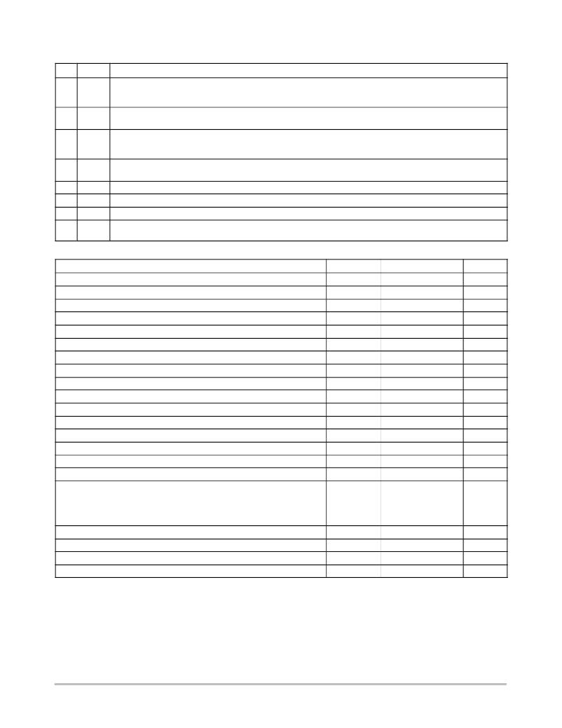
�Table� 1.� PIN� FUNCTION� DESCRIPTION�
�Pin�
�1�
�2�
�3�
�4�
�5�
�6�
�7�
�8�
�Name�
�FB�
�Control�
�Ct�
�CS�
�ZCD�
�GND�
�DRV�
�V� CC�
�Function�
�The� FB� pin� is� the� inverting� input� of� the� internal� error� amplifier.� A� resistor� divider� scales� the� output� voltage� to� V� REF� to� main-�
�tain� regulation.� The� feedback� voltage� is� used� for� overvoltage� and� undervoltage� protections.� The� controller� is� disabled�
�when� this� pin� is� forced� to� a� voltage� less� than� V� UVP� ,� a� voltage� greater� than� V� OVP� ,� or� floating.�
�The� Control� pin� is� the� output� of� the� internal� error� amplifier.� A� compensation� network� is� connected� between� the� Control� pin�
�and� ground� to� set� the� loop� bandwidth.� A� low� bandwidth� yields� a� high� power� factor� and� a� low� Total� Harmonic� Distortion� (THD).�
�The� Ct� pin� sources� a� current� to� charge� an� external� timing� capacitor.� The� circuit� controls� the� power� switch� on� time� by� com-�
�paring� the� Ct� voltage� to� an� internal� voltage� derived� from� V� Control� .� The� Ct� pin� discharges� the� external� timing� capacitor� at� the�
�end� of� the� on� time.�
�The� CS� pin� limits� the� cycle� ?� by� ?� cycle� current� through� the� power� switch.� When� the� CS� voltage� exceeds� V� ILIM� ,� the� drive�
�turns� off.� The� sense� resistor� that� connects� to� the� CS� pin� programs� the� maximum� switch� current.�
�The� voltage� of� an� auxiliary� winding� is� sensed� by� this� pin� to� detect� the� inductor� demagnetization� for� CrM� operation.�
�The� GND� pin� is� analog� ground.�
�The� integrated� driver� has� a� typical� source� impedance� of� 12� W� and� a� typical� sink� impedance� of� 6� W� .�
�The� V� CC� pin� is� the� positive� supply� of� the� controller.� The� controller� is� enabled� when� V� CC� exceeds� V� CC(on)� and� is� disabled�
�when� V� CC� decreases� to� less� than� V� CC(off)� .�
�Table� 2.� MAXIMUM� RATINGS�
�Rating�
�FB� Voltage�
�FB� Current�
�Control� Voltage�
�Control� Current�
�Ct� Voltage�
�Ct� Current�
�CS� Voltage�
�CS� Current�
�ZCD� Voltage�
�ZCD� Current�
�DRV� Voltage�
�DRV� Sink� Current�
�DRV� Source� Current�
�Supply� Voltage�
�Supply� Current�
�Power� Dissipation� (T� A� =� 70� °� C,� 2.0� Oz� Cu,� 55� mm� 2� Printed� Circuit� Copper� Clad)�
�Thermal� Resistance� Junction� ?� to� ?� Ambient�
�(2.0� Oz� Cu,� 55� mm� 2� Printed� Circuit� Copper� Clad)�
�Junction� ?� to� ?� Air,� Low� conductivity� PCB� (Note� 3)�
�Junction� ?� to� ?� Air,� High� conductivity� PCB� (Note� 4)�
�Operating� Junction� Temperature� Range�
�Maximum� Junction� Temperature�
�Storage� Temperature� Range�
�Lead� Temperature� (Soldering,� 10� s)�
�Symbol�
�V� FB�
�I� FB�
�V� Control�
�I� Control�
�V� Ct�
�I� Ct�
�V� CS�
�I� CS�
�V� ZCD�
�I� ZCD�
�V� DRV�
�I� DRV(sink)�
�I� DRV(source)�
�V� CC�
�I� CC�
�P� D�
�R� q� JA�
�R� q� JA�
�R� q� JA�
�T� J�
�T� J(MAX)�
�T� STG�
�T� L�
�Value�
�?� 0.3� to� 10�
�±� 10�
�?� 0.3� to� 6.5�
�?� 2� to� 10�
�?� 0.3� to� 6�
�±� 10�
�?� 0.3� to� 6�
�±� 10�
�?� 0.3� to� 10�
�±� 10�
�?� 0.3� to� V� CC�
�800�
�500�
�?� 0.3� to� 20�
�±� 20�
�450�
�178�
�168�
�127�
�?� 40� to� 125�
�150�
�?� 65� to� 150�
�300�
�Unit�
�V�
�mA�
�V�
�mA�
�V�
�mA�
�V�
�mA�
�V�
�mA�
�V�
�mA�
�mA�
�V�
�mA�
�mW�
�°� C/W�
�°� C�
�°� C�
�°� C�
�°� C�
�Stresses� exceeding� Maximum� Ratings� may� damage� the� device.� Maximum� Ratings� are� stress� ratings� only.� Functional� operation� above� the�
�Recommended� Operating� Conditions� is� not� implied.� Extended� exposure� to� stresses� above� the� Recommended� Operating� Conditions� may� affect�
�device� reliability.�
�1.� This� device� series� contains� ESD� protection� and� exceeds� the� following� tests:�
�Pins� 1–� 8:� Human� Body� Model� 2000� V� per� JEDEC� Standard� JESD22� ?� A114E.�
�Pins� 1–� 8:� Machine� Model� Method� 200� V� per� JEDEC� Standard� JESD22� ?� A115� ?� A.�
�2.� This� device� contains� Latch� ?� Up� protection� and� exceeds� ±� 100� mA� per� JEDEC� Standard� JESD78.�
�3.� As� mounted� on� a� 40x40x1.5� mm� FR4� substrate� with� a� single� layer� of� 80� mm� 2� of� 2� oz� copper� traces� and� heat� spreading� area.� As� specified� for�
�a� JEDEC� 51� low� conductivity� test� PCB.� Test� conditions� were� under� natural� convection� or� zero� air� flow.�
�4.� As� mounted� on� a� 40x40x1.5� mm� FR4� substrate� with� a� single� layer� of� 650� mm� 2� of� 2� oz� copper� traces� and� heat� spreading� area.� As� specified�
�for� a� JEDEC� 51� high� conductivity� test� PCB.� Test� conditions� were� under� natural� convection� or� zero� air� flow.�
�http://onsemi.com�
�3�
�相关PDF资料 |
PDF描述 |
|---|---|
| PSA15R-060PV | ADAPTER WALL R-SERIES 15W 6V |
| PSA15R-050PV | ADAPTER WALL R-SERIES 15W 5V |
| 356-025-506-104 | CARDEDGE 25POS .156 BLACK |
| 356-025-506-102 | CARDEDGE 25POS .156 BLACK |
| FAN7527BMX | IC PFC CTRLR TRANSITION 8SOIC |
相关代理商/技术参数 |
参数描述 |
|---|---|
| NCP1608BOOSTGEVB | 功能描述:电源管理IC开发工具 NCP1608 100 W BOOST EVB PWR SPY RoHS:否 制造商:Maxim Integrated 产品:Evaluation Kits 类型:Battery Management 工具用于评估:MAX17710GB 输入电压: 输出电压:1.8 V |
| NCP1611ADR2G | 功能描述:功率因数校正 IC NCP1611A ENHANCED PFC RoHS:否 制造商:Fairchild Semiconductor 开关频率:300 KHz 最大功率耗散: 最大工作温度:+ 125 C 安装风格:SMD/SMT 封装 / 箱体:SOIC-8 封装:Reel |
| NCP1611BDR2G | 功能描述:功率因数校正 IC NCP1611A ENHANCED PFC RoHS:否 制造商:Fairchild Semiconductor 开关频率:300 KHz 最大功率耗散: 最大工作温度:+ 125 C 安装风格:SMD/SMT 封装 / 箱体:SOIC-8 封装:Reel |
| NCP1611GEVB | 制造商:ON Semiconductor 功能描述:PG - ACDC CONVERSION - Bulk 制造商:ON Semiconductor 功能描述:EVAL BOARD, NCP1611, POWER FACTOR CORRECTION; Silicon Manufacturer:On Semiconductor; Silicon Core Number:NCP1611; Kit Application Type:Power Management; Application Sub Type:Power Factor Correction (PFC) ;RoHS Compliant: Yes |
| NCP1612ADR2G | 功能描述:功率因数校正 IC RoHS:否 制造商:Fairchild Semiconductor 开关频率:300 KHz 最大功率耗散: 最大工作温度:+ 125 C 安装风格:SMD/SMT 封装 / 箱体:SOIC-8 封装:Reel |
发布紧急采购,3分钟左右您将得到回复。