- 您现在的位置:买卖IC网 > PDF目录20308 > NCP1608BDR2G (ON Semiconductor)IC PFC CTLR/PRECONVERTER 8-SOIC PDF资料下载
参数资料
| 型号: | NCP1608BDR2G |
| 厂商: | ON Semiconductor |
| 文件页数: | 13/24页 |
| 文件大小: | 0K |
| 描述: | IC PFC CTLR/PRECONVERTER 8-SOIC |
| 标准包装: | 1 |
| 模式: | 临界传导(CRM) |
| 电流 - 启动: | 24µA |
| 电源电压: | 10.2 V ~ 20 V |
| 工作温度: | -40°C ~ 125°C |
| 安装类型: | 表面贴装 |
| 封装/外壳: | 8-SOIC(0.154",3.90mm 宽) |
| 供应商设备封装: | 8-SOICN |
| 包装: | 标准包装 |
| 其它名称: | NCP1608BDR2GOSDKR |
�� �
�
�NCP1608�
�V� out�
�R� out1� +�
�R� out1� @� R� FB�
�R� out2� +�
�V� out�
�V� REF�
�V� out� +� V� REF� @� R� out1� @�
�R� out2� )� R� FB�
�R� out2� @� R� FB�
�A� resistor� divider� (R� out1� and� R� out2� )� scales� down� the� boost�
�output� voltage� (V� out� )� and� is� connected� to� the� FB� pin.� If� the�
�output� voltage� is� less� than� the� target� output� voltage,� then�
�V� FB� is� less� than� V� REF� and� the� EA� increases� the� control�
�voltage� (V� Control� ).� This� increases� the� on� time� of� the� driver,�
�which� increases� the� power� delivered� to� the� output.� The�
�increase� in� delivered� power� causes� V� out� to� increase� until� the�
�target� output� voltage� is� achieved.� Alternatively,� if� V� out� is�
�greater� than� the� target� output� voltage,� then� V� Control�
�decreases� to� cause� the� on� time� to� decrease� until� V� out�
�decreases� to� the� target� output� voltage.� This� cause� and� effect�
�regulates� V� out� so� that� the� scaled� down� V� out� that� is� applied�
�to� FB� through� R� out1� and� R� out2� is� equal� to� V� REF� .� The�
�presence� of� R� FB� (4.6� M� W� typical� value)� for� FPP� is� included�
�in� the� divider� network� calculation.�
�The� output� voltage� is� set� using� Equation� 2:�
�)� 1� (eq.� 2)�
�The� divider� network� bias� current� is� selected� to� optimize�
�the� tradeoff� of� noise� immunity� and� power� dissipation.� R� out1�
�is� calculated� using� the� bias� current� and� output� voltage� using�
�(eq.� 3)�
�I� bias(out)�
�Where� I� bias(out)� is� the� output� divider� network� bias� current.�
�R� out2� is� dependent� on� V� out� ,� R� out1� ,� and� R� FB� .�
�R� out2� is� calculated� using� Equation� 4:�
�(eq.� 4)�
�R� FB� @� *� 1� *� R� out1�
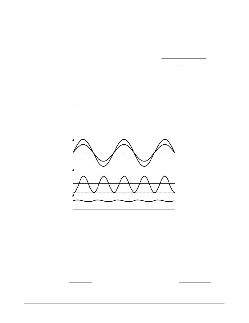
�The� PFC� stage� consumes� a� sinusoidal� current� from� a�
�sinusoidal� line� voltage.� The� converter� provides� the� load�
�with� a� power� that� matches� the� average� demand� only.� The�
�output� capacitor� (C� bulk� )� compensates� for� the� difference�
�between� the� delivered� power� and� the� power� consumed� by�
�the� load.� When� the� power� delivered� to� the� load� is� less� than�
�the� power� consumed� by� the� load,� C� bulk� discharges.� When�
�the� delivered� power� is� greater� than� the� power� consumed� by�
�the� load,� C� bulk� charges� to� store� the� excess� energy.� The�
�situation� is� depicted� in� Figure� 30.�
�Equation� 3:�
�Iac�
�Vac�
�P� in�
�P� out�
�V� out�
�Figure� 30.� Output� Voltage� Ripple� for� a� Constant� Output� Power�
�C� COMP� +�
�2� @� p� @� f� CROSS�
�V� Ct(off)� +� V� Control� ?� Ct� (offset)� +� (eq.� 6)�
�Due� to� the� charging/discharging� of� C� bulk� ,� V� out� contains�
�a� ripple� at� a� frequency� of� either� 100� Hz� (for� a� 50� Hz� line�
�frequency� in� Europe)� or� 120� Hz� (for� a� 60� Hz� line� frequency�
�in� the� USA).� The� V� out� ripple� is� attenuated� by� the� regulation�
�loop� to� ensure� V� Control� is� constant� during� the� ac� line� cycle�
�for� the� proper� shaping� of� the� line� current.� To� ensure� V� Control�
�is� constant� during� the� ac� line� cycle,� the� loop� bandwidth� is�
�typically� set� below� 20� Hz.� A� type� 1� compensation� network�
�consists� of� a� capacitor� (C� COMP� )� connected� between� the�
�Control� and� ground� pins� (see� Figure� 1).� The� capacitor� value�
�that� sets� the� loop� bandwidth� is� calculated� using� Equation� 5:�
�gm�
�(eq.� 5)�
�Where� f� CROSS� is� the� crossover� frequency� and� gm� is� the�
�error� amplifier� transconductance.� The� crossover� frequency�
�is� set� below� 20� Hz.�
�On� Time� Sequence�
�The� switching� pattern� consists� of� constant� on� times� and�
�variable� off� times� for� a� given� rms� input� voltage� and� output�
�load.� The� NCP1608� controls� the� on� time� with� the� capacitor�
�connected� to� the� Ct� pin.� A� current� source� charges� the� Ct�
�capacitor� to� a� voltage� derived� from� the� Control� pin� voltage�
�(V� Ct(off)� ).� V� Ct(off)� is� calculated� using� Equation� 6:�
�2� @� P� out� @� L� @� I� charge�
�h� @� Vac� 2� @� Ct�
�When� V� Ct(off)� is� reached,� the� drive� turns� off� (Figure� 31).�
�http://onsemi.com�
�13�
�相关PDF资料 |
PDF描述 |
|---|---|
| PSA15R-060PV | ADAPTER WALL R-SERIES 15W 6V |
| PSA15R-050PV | ADAPTER WALL R-SERIES 15W 5V |
| 356-025-506-104 | CARDEDGE 25POS .156 BLACK |
| 356-025-506-102 | CARDEDGE 25POS .156 BLACK |
| FAN7527BMX | IC PFC CTRLR TRANSITION 8SOIC |
相关代理商/技术参数 |
参数描述 |
|---|---|
| NCP1608BOOSTGEVB | 功能描述:电源管理IC开发工具 NCP1608 100 W BOOST EVB PWR SPY RoHS:否 制造商:Maxim Integrated 产品:Evaluation Kits 类型:Battery Management 工具用于评估:MAX17710GB 输入电压: 输出电压:1.8 V |
| NCP1611ADR2G | 功能描述:功率因数校正 IC NCP1611A ENHANCED PFC RoHS:否 制造商:Fairchild Semiconductor 开关频率:300 KHz 最大功率耗散: 最大工作温度:+ 125 C 安装风格:SMD/SMT 封装 / 箱体:SOIC-8 封装:Reel |
| NCP1611BDR2G | 功能描述:功率因数校正 IC NCP1611A ENHANCED PFC RoHS:否 制造商:Fairchild Semiconductor 开关频率:300 KHz 最大功率耗散: 最大工作温度:+ 125 C 安装风格:SMD/SMT 封装 / 箱体:SOIC-8 封装:Reel |
| NCP1611GEVB | 制造商:ON Semiconductor 功能描述:PG - ACDC CONVERSION - Bulk 制造商:ON Semiconductor 功能描述:EVAL BOARD, NCP1611, POWER FACTOR CORRECTION; Silicon Manufacturer:On Semiconductor; Silicon Core Number:NCP1611; Kit Application Type:Power Management; Application Sub Type:Power Factor Correction (PFC) ;RoHS Compliant: Yes |
| NCP1612ADR2G | 功能描述:功率因数校正 IC RoHS:否 制造商:Fairchild Semiconductor 开关频率:300 KHz 最大功率耗散: 最大工作温度:+ 125 C 安装风格:SMD/SMT 封装 / 箱体:SOIC-8 封装:Reel |
发布紧急采购,3分钟左右您将得到回复。