- 您现在的位置:买卖IC网 > Datasheet目录488 > NTGD3148NT1G (ON Semiconductor)MOSFET N-CH DUAL 20V 3.5A 6TSOP Datasheet资料下载
参数资料
| 型号: | NTGD3148NT1G |
| 厂商: | ON Semiconductor |
| 文件页数: | 1/5页 |
| 文件大小: | 0K |
| 描述: | MOSFET N-CH DUAL 20V 3.5A 6TSOP |
| 标准包装: | 1 |
| FET 型: | 2 个 N 沟道(双) |
| FET 特点: | 逻辑电平门 |
| 漏极至源极电压(Vdss): | 20V |
| 电流 - 连续漏极(Id) @ 25° C: | 3A |
| 开态Rds(最大)@ Id, Vgs @ 25° C: | 70 毫欧 @ 3.5A,4.5V |
| Id 时的 Vgs(th)(最大): | 1.5V @ 250µA |
| 闸电荷(Qg) @ Vgs: | 3.8nC @ 4.5V |
| 输入电容 (Ciss) @ Vds: | 300pF @ 10V |
| 功率 - 最大: | 900mW |
| 安装类型: | 表面贴装 |
| 封装/外壳: | SC-74,SOT-457 |
| 供应商设备封装: | 6-TSOP |
| 包装: | 标准包装 |
| 其它名称: | NTGD3148NT1GOSDKR |
�� �
�
�NTGD3148N�
�Power� MOSFET�
�20� V,� 3.5� A,� Dual� N-Channel,� TSOP-6�
�Features�
�?� Low� Threshold� Levels,� VGS(th)� <� 1.5� V�
�?� Low� Gate� Charge� (3.8� nC)�
�?� Leading� Edge� Trench� Technology� of� Low� R� DS(on)�
�?� High� Power� and� Current� Handling� Capability�
�?� This� is� a� Pb-Free� Device�
�Applications�
�?� DC-DC� Converters� (Buck� and� Boost� Circuits)�
�?� Low� Side� Load� Switch�
�?� Optimized� for� Battery� and� Load� Management� Applications� in�
�Portable� Equipment� Like� Cell� Phones,� DSCs,� Media� Player,� Etc�
�?�
�Battery� Charging� and� Protection� Circuits�
�MAXIMUM� RATINGS� (T� J� =� 25� °� C� unless� otherwise� noted)�
�V� (BR)DSS�
�20� V�
�http://onsemi.com�
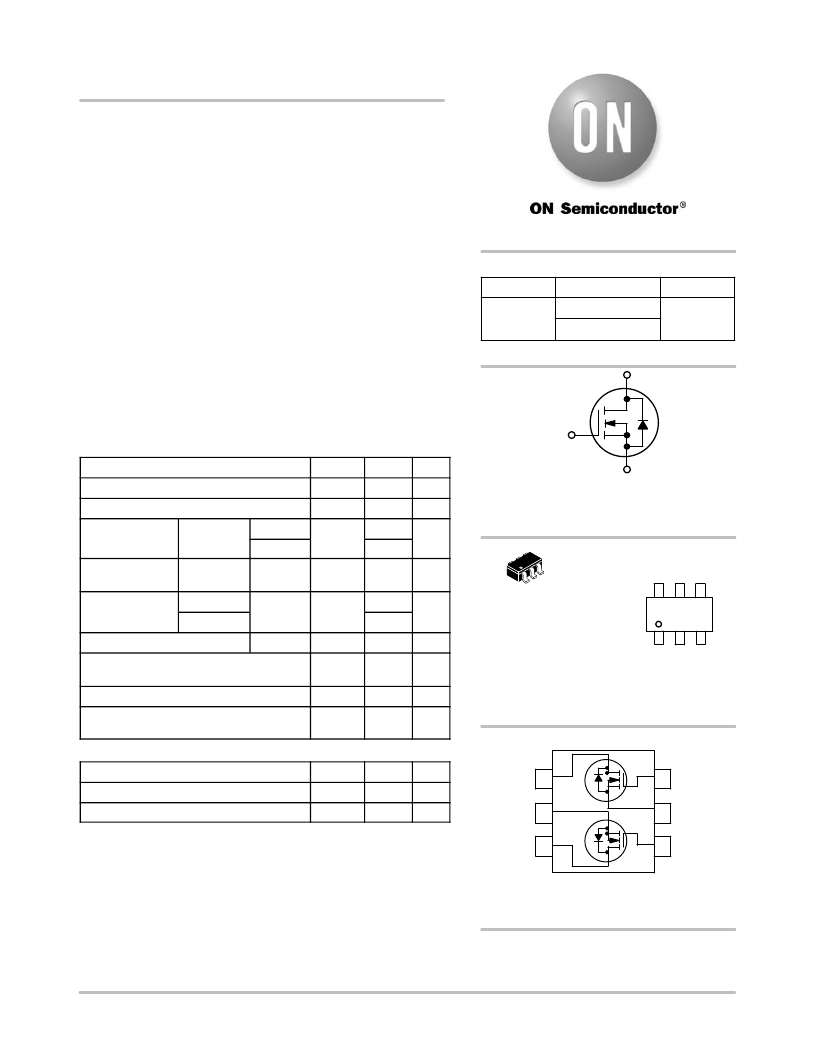
�N-CHANNEL� MOSFET�
�R� DS(on)� Max�
�70� m� W� @� 4.5� V�
�100� m� W� @� 2.5� V�
�D�
�G�
�I� D� Max�
�3.5� A�
�Parameter�
�Drain-to-Source� Voltage�
�Gate-to-Source� Voltage�
�Symbol�
�V� DSS�
�V� GS�
�Value�
�20�
�±� 12�
�Unit�
�V�
�V�
�S�
�N-CHANNEL� MOSFET�
�Continuous� Drain�
�Current� (Note� 1)�
�Continuous� Drain�
�Steady� State�
�t� ≤� 5� s�
�T� A� =� 25� °� C�
�T� A� =� 85� °� C�
�T� A� =� 25� °� C�
�I� D�
�I� D�
�3.0�
�2.2�
�3.5�
�A�
�A�
�MARKING�
�DIAGRAM�
�Current� (Note� 1)�
�Power� Dissipation�
�(Note� 1)�
�Steady� State�
�t� ≤� 5� s�
�T� A� =� 25� °� C�
�P� D�
�0.9�
�1.1�
�W�
�1�
�TSOP-6�
�CASE� 318G�
�DN� M� G�
�G�
�Pulsed� Drain� Current�
�t� p� =� 10� m� s�
�I� DM�
�10�
�A�
�STYLE� 13�
�1�
�Operating� Junction� and� Storage� Temperature�
�T� J� ,� T� STG�
�-50� to�
�150�
�°� C�
�DN� =� Specific� Device� Code�
�M� =� Date� Code�
�Source� Current� (Body� Diode)�
�I� S�
�0.8�
�A�
�G�
�=� Pb-Free� Package�
�Lead� Temperature� for� Soldering� Purposes�
�(1/8� ″� from� case� for� 10� s)�
�THERMAL� RESISTANCE� RATINGS�
�T� L�
�260�
�°� C�
�(Note:� Microdot� may� be� in� either� location)�
�PIN� CONNECTION�
�Parameter�
�Junction-to-Ambient� –� Steady� State� (Note� 1)�
�Junction-to-Ambient� –� t� ≤� 5� s� (Note� 1)�
�Symbol�
�R� q� JA�
�R� q� JA�
�Value�
�140�
�110�
�Unit�
�°� C/W�
�°� C/W�
�D� 2�
�S� 1�
�4�
�5�
�3� G� 2�
�2� S� 2�
�Stresses� exceeding� Maximum� Ratings� may� damage� the� device.� Maximum�
�Ratings� are� stress� ratings� only.� Functional� operation� above� the� Recommended�
�Operating� Conditions� is� not� implied.� Extended� exposure� to� stresses� above� the�
�D� 1�
�6�
�1� G� 1�
�Recommended� Operating� Conditions� may� affect� device� reliability.�
�1.� Surface� Mounted� on� FR4� Board� using� 1� in� sq� pad� size� (Cu� area� =� 1.127� in� sq�
�[1� oz]� including� traces).�
�(Top� View)�
�ORDERING� INFORMATION�
�See� detailed� ordering� and� shipping� information� in� the� package�
�dimensions� section� on� page� 2� of� this� data� sheet.�
�?� Semiconductor� Components� Industries,� LLC,� 2008�
�April,� 2008� -� Rev.� 0�
�1�
�Publication� Order� Number:�
�NTGD3148N/D�
�相关PDF资料 |
PDF描述 |
|---|---|
| NTGD3149CT1G | MOSFET COMPL 20V DUAL 6-TSOP |
| NTGD4161PT1G | MOSFET P-CH DUAL 30V 2.3A 6-TSOP |
| NTGD4167CT1G | MOSFET N/P-CH 30V DUAL 6-TSOP |
| NTGD4169FT1G | MOSFET N-CH 30V 2.6A 6-TSOP |
| NTGS1135PT1G | MOSFET P-CH 8V 4.6A 6-TSOP |
相关代理商/技术参数 |
参数描述 |
|---|---|
| NTGD3149C | 制造商:ONSEMI 制造商全称:ON Semiconductor 功能描述:Power MOSFET Complementary, 20 V, +3.5/−2.7 A, TSOP−6 Dual |
| NTGD3149CT1G | 功能描述:MOSFET COMP TSOP6 20V 3A TR RoHS:否 制造商:STMicroelectronics 晶体管极性:N-Channel 汲极/源极击穿电压:650 V 闸/源击穿电压:25 V 漏极连续电流:130 A 电阻汲极/源极 RDS(导通):0.014 Ohms 配置:Single 最大工作温度: 安装风格:Through Hole 封装 / 箱体:Max247 封装:Tube |
| NTGD4161P | 制造商:ONSEMI 制造商全称:ON Semiconductor 功能描述:Power MOSFET -30 V, -2.3 A, Dual P-Channel, TSOP-6 |
| NTGD4161P_06 | 制造商:ONSEMI 制造商全称:ON Semiconductor 功能描述:Power MOSFET -30 V, -2.3 A, Dual P-Channel, TSOP-6 |
| NTGD4161PT1G | 功能描述:MOSFET PFET TSOP6 20V 2.3A 160mOhm RoHS:否 制造商:STMicroelectronics 晶体管极性:N-Channel 汲极/源极击穿电压:650 V 闸/源击穿电压:25 V 漏极连续电流:130 A 电阻汲极/源极 RDS(导通):0.014 Ohms 配置:Single 最大工作温度: 安装风格:Through Hole 封装 / 箱体:Max247 封装:Tube |
发布紧急采购,3分钟左右您将得到回复。