- 您现在的位置:买卖IC网 > PDF目录189448 > OR3L225B7PS432-DB (LATTICE SEMICONDUCTOR CORP) FPGA, 1444 CLBS, 166000 GATES, 266.4 MHz, PBGA432 PDF资料下载
参数资料
| 型号: | OR3L225B7PS432-DB |
| 厂商: | LATTICE SEMICONDUCTOR CORP |
| 元件分类: | FPGA |
| 英文描述: | FPGA, 1444 CLBS, 166000 GATES, 266.4 MHz, PBGA432 |
| 封装: | EBGA-432 |
| 文件页数: | 2/77页 |
| 文件大小: | 873K |
| 代理商: | OR3L225B7PS432-DB |
第1页当前第2页第3页第4页第5页第6页第7页第8页第9页第10页第11页第12页第13页第14页第15页第16页第17页第18页第19页第20页第21页第22页第23页第24页第25页第26页第27页第28页第29页第30页第31页第32页第33页第34页第35页第36页第37页第38页第39页第40页第41页第42页第43页第44页第45页第46页第47页第48页第49页第50页第51页第52页第53页第54页第55页第56页第57页第58页第59页第60页第61页第62页第63页第64页第65页第66页第67页第68页第69页第70页第71页第72页第73页第74页第75页第76页第77页
10
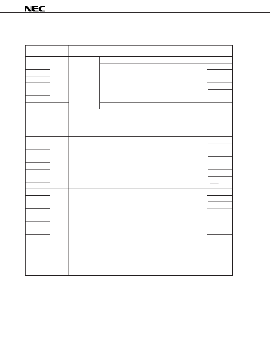
PD78052, 78053, 78054, 78055, 78056, 78058
Data Sheet U12327EJ5V0DS00
3.
PIN FUNCTIONS
3.1 Port Pins (1/2)
Pin Name
I/O
Function
After
Alternate
Reset
Function
P00
Input
Port 0
Input only
Input
INTP0/TI00
P01
I/O
8-bit I/O port
Input/output can be specified in 1-bit units.
Input
INTP1/TI01
P02
When used as an input port, a pull-up resistor can be
INTP2
P03
specified by means of software.
INTP3
P04
INTP4
P05
INTP5
P06
INTP6
P07Note 1
Input
Input only
Input
XT1
P10 to P17
I/O
Port 1
Input
ANI0 to ANI7
8-bit I/O port.
Input/output can be specified in 1-bit units.
When used as an input port, a pull-up resistor can be specified by means
of softwareNote 2.
P20
I/O
Port 2
Input
SI1
P21
8-bit I/O port.
SO1
P22
Input/output can be specified in 1-bit units.
SCK1
P23
When used as an input port, a pull-up resistor can be specified by means
STB
P24
of software.
BUSY
P25
SI0/SB0
P26
SO0/SB1
P27
SCK0
P30
I/O
Port 3
Input
TO0
P31
8-bit I/O port.
TO1
P32
Input/output can be specified in 1-bit units.
TO2
P33
When used as an input port, a pull-up resistor can be specified by means
TI1
P34
of software.
TI2
P35
PCL
P36
BUZ
P37
—
P40 to P47
I/O
Port 4
Input
AD0 to AD7
8-bit I/O port.
Input/output can be specified in 8-bit units.
When used as an input port, a pull-up resistor can be specified by means
of software.
The test input flag (KRIF) is set to 1 by falling edge detection.
Notes 1. When using the P07/XT1 pin as an input port, set bit 6 (FRC) of the processor clock control register (PCC)
to 1. Do not use the on-chip feedback resistor of the subsystem clock oscillator.
2. When using the P10/ANI0 to P17/ANI7 pins as A/D converter analog input pins, set port 1 to the input mode.
At this time, pull-up resistors are automatically disconnected.
相关PDF资料 |
PDF描述 |
|---|---|
| OR3L225B7PS432I-DB | FPGA, 1444 CLBS, 166000 GATES, 266.4 MHz, PBGA432 |
| OR3L225B7PS680-DB | FPGA, 1444 CLBS, 166000 GATES, 266.4 MHz, PBGA680 |
| OR3L225B7PS680I-DB | FPGA, 1444 CLBS, 166000 GATES, 266.4 MHz, PBGA680 |
| OR3L225B8PS432-DB | FPGA, 1444 CLBS, 166000 GATES, 333 MHz, PBGA432 |
| OR3L225B8PS680-DB | FPGA, 1444 CLBS, 166000 GATES, 333 MHz, PBGA680 |
相关代理商/技术参数 |
参数描述 |
|---|---|
| OR3L225B8BC432-DB | 功能描述:FPGA - 现场可编程门阵列 11552 LUT 612 I/O RoHS:否 制造商:Altera Corporation 系列:Cyclone V E 栅极数量: 逻辑块数量:943 内嵌式块RAM - EBR:1956 kbit 输入/输出端数量:128 最大工作频率:800 MHz 工作电源电压:1.1 V 最大工作温度:+ 70 C 安装风格:SMD/SMT 封装 / 箱体:FBGA-256 |
| OR3L225B8BM680-DB | 功能描述:FPGA - 现场可编程门阵列 11552 LUT 612 I/O RoHS:否 制造商:Altera Corporation 系列:Cyclone V E 栅极数量: 逻辑块数量:943 内嵌式块RAM - EBR:1956 kbit 输入/输出端数量:128 最大工作频率:800 MHz 工作电源电压:1.1 V 最大工作温度:+ 70 C 安装风格:SMD/SMT 封装 / 箱体:FBGA-256 |
| OR3LP26B | 制造商:AGERE 制造商全称:AGERE 功能描述:Field-Programmable System Chip (FPSC) Embedded Master/Target PCI Interface |
| OR3LP26BBA352-DB | 功能描述:FPGA - 现场可编程门阵列 FPSC PCI INTERFACE RoHS:否 制造商:Altera Corporation 系列:Cyclone V E 栅极数量: 逻辑块数量:943 内嵌式块RAM - EBR:1956 kbit 输入/输出端数量:128 最大工作频率:800 MHz 工作电源电压:1.1 V 最大工作温度:+ 70 C 安装风格:SMD/SMT 封装 / 箱体:FBGA-256 |
| OR3LP26BBM680-DB | 功能描述:FPGA - 现场可编程门阵列 FPSC PCI INTERFACE RoHS:否 制造商:Altera Corporation 系列:Cyclone V E 栅极数量: 逻辑块数量:943 内嵌式块RAM - EBR:1956 kbit 输入/输出端数量:128 最大工作频率:800 MHz 工作电源电压:1.1 V 最大工作温度:+ 70 C 安装风格:SMD/SMT 封装 / 箱体:FBGA-256 |
发布紧急采购,3分钟左右您将得到回复。