- 您现在的位置:买卖IC网 > PDF目录189448 > OR3L225B7PS432-DB (LATTICE SEMICONDUCTOR CORP) FPGA, 1444 CLBS, 166000 GATES, 266.4 MHz, PBGA432 PDF资料下载
参数资料
| 型号: | OR3L225B7PS432-DB |
| 厂商: | LATTICE SEMICONDUCTOR CORP |
| 元件分类: | FPGA |
| 英文描述: | FPGA, 1444 CLBS, 166000 GATES, 266.4 MHz, PBGA432 |
| 封装: | EBGA-432 |
| 文件页数: | 21/77页 |
| 文件大小: | 873K |
| 代理商: | OR3L225B7PS432-DB |
第1页第2页第3页第4页第5页第6页第7页第8页第9页第10页第11页第12页第13页第14页第15页第16页第17页第18页第19页第20页当前第21页第22页第23页第24页第25页第26页第27页第28页第29页第30页第31页第32页第33页第34页第35页第36页第37页第38页第39页第40页第41页第42页第43页第44页第45页第46页第47页第48页第49页第50页第51页第52页第53页第54页第55页第56页第57页第58页第59页第60页第61页第62页第63页第64页第65页第66页第67页第68页第69页第70页第71页第72页第73页第74页第75页第76页第77页
28
PD78052, 78053, 78054, 78055, 78056, 78058
Data Sheet U12327EJ5V0DS00
6. INTERRUPT FUNCTIONS AND TEST FUNCTIONS
6.1 Interrupt Functions
A total of 22 interrupt sources are provided, divided into the following three types.
Non-maskable: 1
Maskable:
20
Software:
1
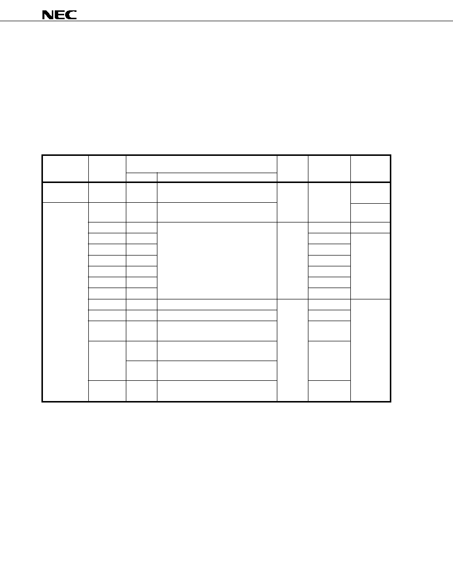
The following table shows the interrupt source list.
Table 6-1. Interrupt Source List (1/2)
Default
Interrupt Source
Internal/
Vector
Basic
Interrupt Type
Table
Configuration
PriorityNote 1
Name
Trigger
External
Address
TypeNote 2
Non-maskable
—
INTWDT
Watchdog timer overflow
Internal
0004H
(A)
(with watchdog timer mode 1 selected)
Maskable
0
INTWDT
Watchdog timer overflow
(B)
(with interval timer mode selected)
1
INTP0
Pin input edge detection
External
0006H
(C)
2
INTP1
0008H
(D)
3
INTP2
000AH
4
INTP3
000CH
5
INTP4
000EH
6
INTP5
0010H
7
INTP6
0012H
8
INTCSI0
End of serial interface channel 0 transfer
Internal
0014H
(B)
9
INTCSI1
End of serial interface channel 1 transfer
0016H
10
INTSER
Occurrence of serial interface channel 2
0018H
UART reception error
11
INTSR
End of serial interface channel 2 UART
001AH
reception
INTCSI2
End of serial interface channel 2 3-wire
transfer
12
INTST
End of serial interface channel 2 UART
001CH
transmission
Notes 1. Default priority is the priority order when several maskable interrupt requests are generated at the same
time. 0 is the highest and 18 is the lowest.
2. Basic configuration types (A) to (E) correspond to (A) to (E) in Figure 6-1.
相关PDF资料 |
PDF描述 |
|---|---|
| OR3L225B7PS432I-DB | FPGA, 1444 CLBS, 166000 GATES, 266.4 MHz, PBGA432 |
| OR3L225B7PS680-DB | FPGA, 1444 CLBS, 166000 GATES, 266.4 MHz, PBGA680 |
| OR3L225B7PS680I-DB | FPGA, 1444 CLBS, 166000 GATES, 266.4 MHz, PBGA680 |
| OR3L225B8PS432-DB | FPGA, 1444 CLBS, 166000 GATES, 333 MHz, PBGA432 |
| OR3L225B8PS680-DB | FPGA, 1444 CLBS, 166000 GATES, 333 MHz, PBGA680 |
相关代理商/技术参数 |
参数描述 |
|---|---|
| OR3L225B8BC432-DB | 功能描述:FPGA - 现场可编程门阵列 11552 LUT 612 I/O RoHS:否 制造商:Altera Corporation 系列:Cyclone V E 栅极数量: 逻辑块数量:943 内嵌式块RAM - EBR:1956 kbit 输入/输出端数量:128 最大工作频率:800 MHz 工作电源电压:1.1 V 最大工作温度:+ 70 C 安装风格:SMD/SMT 封装 / 箱体:FBGA-256 |
| OR3L225B8BM680-DB | 功能描述:FPGA - 现场可编程门阵列 11552 LUT 612 I/O RoHS:否 制造商:Altera Corporation 系列:Cyclone V E 栅极数量: 逻辑块数量:943 内嵌式块RAM - EBR:1956 kbit 输入/输出端数量:128 最大工作频率:800 MHz 工作电源电压:1.1 V 最大工作温度:+ 70 C 安装风格:SMD/SMT 封装 / 箱体:FBGA-256 |
| OR3LP26B | 制造商:AGERE 制造商全称:AGERE 功能描述:Field-Programmable System Chip (FPSC) Embedded Master/Target PCI Interface |
| OR3LP26BBA352-DB | 功能描述:FPGA - 现场可编程门阵列 FPSC PCI INTERFACE RoHS:否 制造商:Altera Corporation 系列:Cyclone V E 栅极数量: 逻辑块数量:943 内嵌式块RAM - EBR:1956 kbit 输入/输出端数量:128 最大工作频率:800 MHz 工作电源电压:1.1 V 最大工作温度:+ 70 C 安装风格:SMD/SMT 封装 / 箱体:FBGA-256 |
| OR3LP26BBM680-DB | 功能描述:FPGA - 现场可编程门阵列 FPSC PCI INTERFACE RoHS:否 制造商:Altera Corporation 系列:Cyclone V E 栅极数量: 逻辑块数量:943 内嵌式块RAM - EBR:1956 kbit 输入/输出端数量:128 最大工作频率:800 MHz 工作电源电压:1.1 V 最大工作温度:+ 70 C 安装风格:SMD/SMT 封装 / 箱体:FBGA-256 |
发布紧急采购,3分钟左右您将得到回复。