- 您现在的位置:买卖IC网 > PDF目录189448 > OR3L225B7PS432-DB (LATTICE SEMICONDUCTOR CORP) FPGA, 1444 CLBS, 166000 GATES, 266.4 MHz, PBGA432 PDF资料下载
参数资料
| 型号: | OR3L225B7PS432-DB |
| 厂商: | LATTICE SEMICONDUCTOR CORP |
| 元件分类: | FPGA |
| 英文描述: | FPGA, 1444 CLBS, 166000 GATES, 266.4 MHz, PBGA432 |
| 封装: | EBGA-432 |
| 文件页数: | 42/77页 |
| 文件大小: | 873K |
| 代理商: | OR3L225B7PS432-DB |
第1页第2页第3页第4页第5页第6页第7页第8页第9页第10页第11页第12页第13页第14页第15页第16页第17页第18页第19页第20页第21页第22页第23页第24页第25页第26页第27页第28页第29页第30页第31页第32页第33页第34页第35页第36页第37页第38页第39页第40页第41页当前第42页第43页第44页第45页第46页第47页第48页第49页第50页第51页第52页第53页第54页第55页第56页第57页第58页第59页第60页第61页第62页第63页第64页第65页第66页第67页第68页第69页第70页第71页第72页第73页第74页第75页第76页第77页
47
PD78052, 78053, 78054, 78055, 78056, 78058
Data Sheet U12327EJ5V0DS00
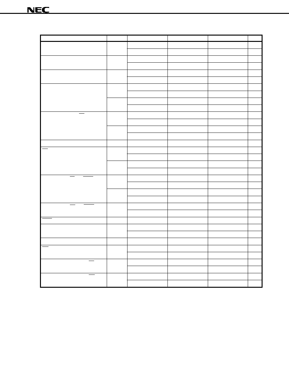
(b) Except when MCS = 1, PCC2 to PCC0 = 000B (TA = –40 to +85
°C, VDD = 2.0 to 6.0 V)
Parameter
Symbol
Conditions
MIN.
MAX.
Unit
ASTB high-level width
tASTH
VDD = 2.7 to 6.0 V
tCY – 80
ns
tCY – 150
ns
Address setup time
tADS
VDD = 2.7 to 6.0 V
tCY – 80
ns
tCY – 150
ns
Address hold time
tADH
VDD = 2.7 to 6.0 V
0.4tCY – 10
ns
0.37tCY – 40
ns
Data input time from address
tADD1
VDD = 2.7 to 6.0 V
(3 + 2n)tCY – 160
ns
(3 + 2n)tCY – 320
ns
tADD2
VDD = 2.7 to 6.0 V
(4 + 2n)tCY – 200
ns
(4 + 2n)tCY – 300
ns
Data input time from RD
↓
tRDD1
VDD = 2.7 to 6.0 V
(1.4 + 2n)tCY – 70
ns
(1.37 + 2n)tCY – 120
ns
tRDD2
VDD = 2.7 to 6.0 V
(2.4 + 2n)tCY – 70
ns
(2.37 + 2n)tCY – 120
ns
Read data hold time
tRDH
0ns
RD low-level width
tRDL1
VDD = 2.7 to 6.0 V
(1.4 + 2n)tCY – 20
ns
(1.37 + 2n)tCY – 20
ns
tRDL2
VDD = 2.7 to 6.0 V
(2.4 + 2n)tCY – 20
ns
(2.37 + 2n)tCY – 20
ns
Input time from RD
↓ to WAIT↓
tRDWT1
VDD = 2.7 to 6.0 V
tCY – 100
ns
tCY – 200
ns
tRDWT2
VDD = 2.7 to 6.0 V
2tCY – 100
ns
2tCY – 200
ns
Input time from WR
↓ to WAIT↓
tWRWT
VDD = 2.7 to 6.0 V
2tCY – 100
ns
2tCY – 200
ns
WAIT low-level width
tWTL
(1 + 2n)tCY
(2 + 2n)tCY
ns
Write data setup time
tWDS
VDD = 2.7 to 6.0 V
(2.4 + 2n)tCY – 60
ns
(2.37 + 2n)tCY – 100
ns
Write data hold time
tWDH
20
ns
WR low-level width
tWRL
VDD = 2.7 to 6.0 V
(2.4 + 2n)tCY – 20
ns
(2.37 + 2n)tCY – 20
ns
Delay time from ASTB
↓ to RD↓
tASTRD
VDD = 2.7 to 6.0 V
0.4tCY – 30
ns
0.37tCY – 50
ns
Delay time from ASTB
↓ to WR↓
tASTWR
VDD = 2.7 to 6.0 V
1.4tCY – 30
ns
1.37tCY – 50
ns
Remarks 1. MCS: Bit 0 of the oscillation mode selection register (OSMS)
2. PCC2 to PCC0: Bits 2 to 0 of the processor clock control register (PCC)
3. tCY = TCY/4
4. n indicates the number of waits.
相关PDF资料 |
PDF描述 |
|---|---|
| OR3L225B7PS432I-DB | FPGA, 1444 CLBS, 166000 GATES, 266.4 MHz, PBGA432 |
| OR3L225B7PS680-DB | FPGA, 1444 CLBS, 166000 GATES, 266.4 MHz, PBGA680 |
| OR3L225B7PS680I-DB | FPGA, 1444 CLBS, 166000 GATES, 266.4 MHz, PBGA680 |
| OR3L225B8PS432-DB | FPGA, 1444 CLBS, 166000 GATES, 333 MHz, PBGA432 |
| OR3L225B8PS680-DB | FPGA, 1444 CLBS, 166000 GATES, 333 MHz, PBGA680 |
相关代理商/技术参数 |
参数描述 |
|---|---|
| OR3L225B8BC432-DB | 功能描述:FPGA - 现场可编程门阵列 11552 LUT 612 I/O RoHS:否 制造商:Altera Corporation 系列:Cyclone V E 栅极数量: 逻辑块数量:943 内嵌式块RAM - EBR:1956 kbit 输入/输出端数量:128 最大工作频率:800 MHz 工作电源电压:1.1 V 最大工作温度:+ 70 C 安装风格:SMD/SMT 封装 / 箱体:FBGA-256 |
| OR3L225B8BM680-DB | 功能描述:FPGA - 现场可编程门阵列 11552 LUT 612 I/O RoHS:否 制造商:Altera Corporation 系列:Cyclone V E 栅极数量: 逻辑块数量:943 内嵌式块RAM - EBR:1956 kbit 输入/输出端数量:128 最大工作频率:800 MHz 工作电源电压:1.1 V 最大工作温度:+ 70 C 安装风格:SMD/SMT 封装 / 箱体:FBGA-256 |
| OR3LP26B | 制造商:AGERE 制造商全称:AGERE 功能描述:Field-Programmable System Chip (FPSC) Embedded Master/Target PCI Interface |
| OR3LP26BBA352-DB | 功能描述:FPGA - 现场可编程门阵列 FPSC PCI INTERFACE RoHS:否 制造商:Altera Corporation 系列:Cyclone V E 栅极数量: 逻辑块数量:943 内嵌式块RAM - EBR:1956 kbit 输入/输出端数量:128 最大工作频率:800 MHz 工作电源电压:1.1 V 最大工作温度:+ 70 C 安装风格:SMD/SMT 封装 / 箱体:FBGA-256 |
| OR3LP26BBM680-DB | 功能描述:FPGA - 现场可编程门阵列 FPSC PCI INTERFACE RoHS:否 制造商:Altera Corporation 系列:Cyclone V E 栅极数量: 逻辑块数量:943 内嵌式块RAM - EBR:1956 kbit 输入/输出端数量:128 最大工作频率:800 MHz 工作电源电压:1.1 V 最大工作温度:+ 70 C 安装风格:SMD/SMT 封装 / 箱体:FBGA-256 |
发布紧急采购,3分钟左右您将得到回复。