- 您现在的位置:买卖IC网 > PDF目录189448 > OR3L225B7PS432-DB (LATTICE SEMICONDUCTOR CORP) FPGA, 1444 CLBS, 166000 GATES, 266.4 MHz, PBGA432 PDF资料下载
参数资料
| 型号: | OR3L225B7PS432-DB |
| 厂商: | LATTICE SEMICONDUCTOR CORP |
| 元件分类: | FPGA |
| 英文描述: | FPGA, 1444 CLBS, 166000 GATES, 266.4 MHz, PBGA432 |
| 封装: | EBGA-432 |
| 文件页数: | 32/77页 |
| 文件大小: | 873K |
| 代理商: | OR3L225B7PS432-DB |
第1页第2页第3页第4页第5页第6页第7页第8页第9页第10页第11页第12页第13页第14页第15页第16页第17页第18页第19页第20页第21页第22页第23页第24页第25页第26页第27页第28页第29页第30页第31页当前第32页第33页第34页第35页第36页第37页第38页第39页第40页第41页第42页第43页第44页第45页第46页第47页第48页第49页第50页第51页第52页第53页第54页第55页第56页第57页第58页第59页第60页第61页第62页第63页第64页第65页第66页第67页第68页第69页第70页第71页第72页第73页第74页第75页第76页第77页
38
PD78052, 78053, 78054, 78055, 78056, 78058
Data Sheet U12327EJ5V0DS00
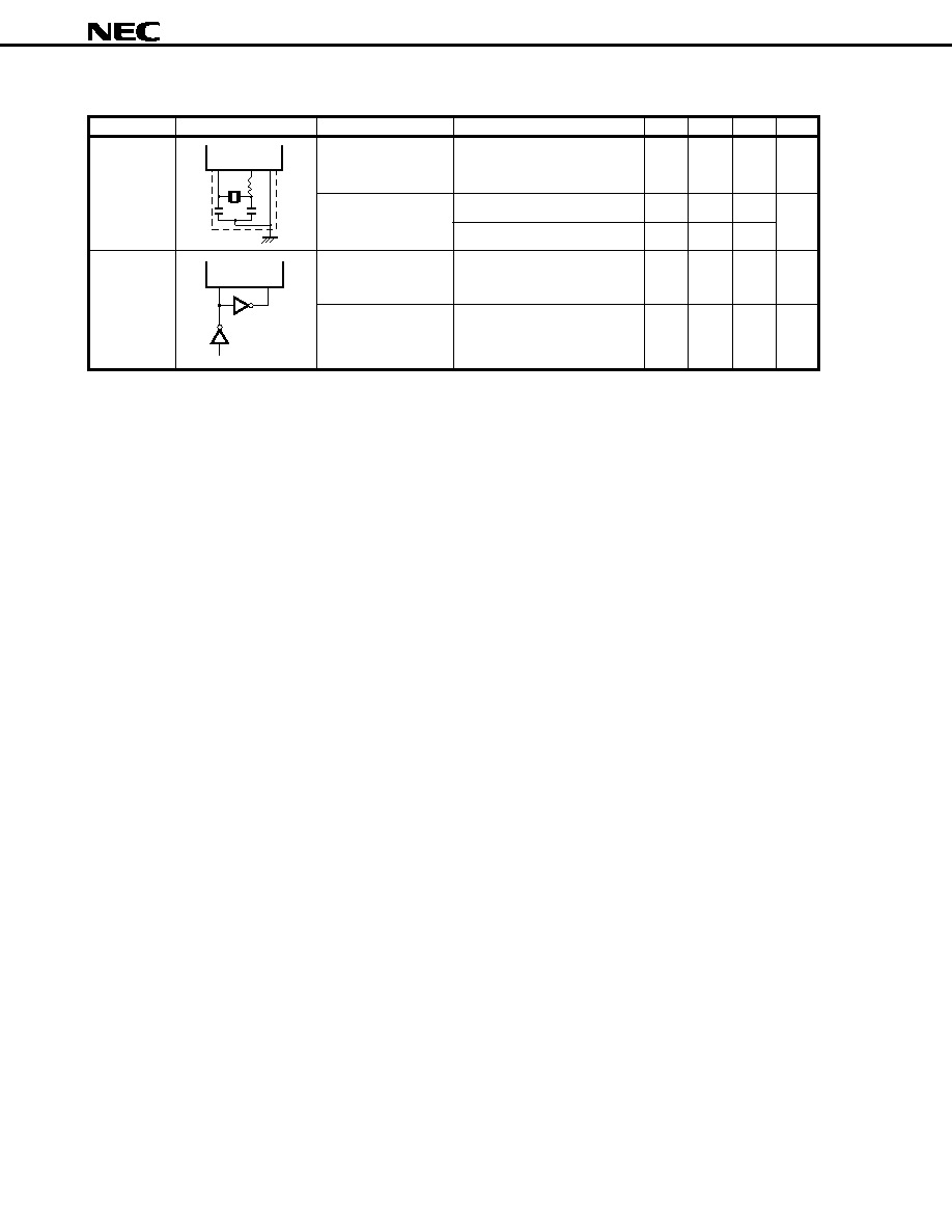
Subsystem Clock Oscillator Characteristics (TA = –40 to +85
°C, VDD = 2.0 to 6.0 V)
Resonator
Recommended Circuit
Parameter
Conditions
MIN.
TYP.
MAX.
Unit
Crystal
Oscillation
32
32.768
35
kHz
resonator
frequency (fXT)Note 1
Oscillation
VDD = 4.5 to 6.0 V
1.2
2
s
stabilization timeNote 2
10
External
XT1 input
32
100
kHz
clock
frequency (fXT)Note 1
XT1 input
5
15
s
high-/low-level width
(tXTH , tXTL)
Notes 1. Indicates only oscillator characteristics. Refer to AC Characteristics for instruction execution time.
2. Time required to stabilize oscillation after VDD reaches oscillation voltage range MIN.
Cautions 1. When using the subsystem clock oscillator, wire as follows in the area enclosed by the broken
lines in the above figures to avoid an adverse effect from wiring capacitance.
Keep the wiring length as short as possible.
Do not cross wiring with the other signal lines.
Do not route the wiring near a signal line through which a high fluctuating current flows.
Always make the ground point of the oscillator capacitor the same potential as VSS.
Do not ground the capacitor to a ground pattern through which a high current flows.
Do not fetch signals from the oscillator.
2. The subsystem clock oscillator is designed as a low-amplitude circuit for reducing current
consumption, and is more prone to malfunction due to noise than the main system clock
oscillator. Particular care is therefore required with the wiring method when the subsystem clock
is used.
XT1 XT2
C4
C3
R2
IC
XT1
XT2
相关PDF资料 |
PDF描述 |
|---|---|
| OR3L225B7PS432I-DB | FPGA, 1444 CLBS, 166000 GATES, 266.4 MHz, PBGA432 |
| OR3L225B7PS680-DB | FPGA, 1444 CLBS, 166000 GATES, 266.4 MHz, PBGA680 |
| OR3L225B7PS680I-DB | FPGA, 1444 CLBS, 166000 GATES, 266.4 MHz, PBGA680 |
| OR3L225B8PS432-DB | FPGA, 1444 CLBS, 166000 GATES, 333 MHz, PBGA432 |
| OR3L225B8PS680-DB | FPGA, 1444 CLBS, 166000 GATES, 333 MHz, PBGA680 |
相关代理商/技术参数 |
参数描述 |
|---|---|
| OR3L225B8BC432-DB | 功能描述:FPGA - 现场可编程门阵列 11552 LUT 612 I/O RoHS:否 制造商:Altera Corporation 系列:Cyclone V E 栅极数量: 逻辑块数量:943 内嵌式块RAM - EBR:1956 kbit 输入/输出端数量:128 最大工作频率:800 MHz 工作电源电压:1.1 V 最大工作温度:+ 70 C 安装风格:SMD/SMT 封装 / 箱体:FBGA-256 |
| OR3L225B8BM680-DB | 功能描述:FPGA - 现场可编程门阵列 11552 LUT 612 I/O RoHS:否 制造商:Altera Corporation 系列:Cyclone V E 栅极数量: 逻辑块数量:943 内嵌式块RAM - EBR:1956 kbit 输入/输出端数量:128 最大工作频率:800 MHz 工作电源电压:1.1 V 最大工作温度:+ 70 C 安装风格:SMD/SMT 封装 / 箱体:FBGA-256 |
| OR3LP26B | 制造商:AGERE 制造商全称:AGERE 功能描述:Field-Programmable System Chip (FPSC) Embedded Master/Target PCI Interface |
| OR3LP26BBA352-DB | 功能描述:FPGA - 现场可编程门阵列 FPSC PCI INTERFACE RoHS:否 制造商:Altera Corporation 系列:Cyclone V E 栅极数量: 逻辑块数量:943 内嵌式块RAM - EBR:1956 kbit 输入/输出端数量:128 最大工作频率:800 MHz 工作电源电压:1.1 V 最大工作温度:+ 70 C 安装风格:SMD/SMT 封装 / 箱体:FBGA-256 |
| OR3LP26BBM680-DB | 功能描述:FPGA - 现场可编程门阵列 FPSC PCI INTERFACE RoHS:否 制造商:Altera Corporation 系列:Cyclone V E 栅极数量: 逻辑块数量:943 内嵌式块RAM - EBR:1956 kbit 输入/输出端数量:128 最大工作频率:800 MHz 工作电源电压:1.1 V 最大工作温度:+ 70 C 安装风格:SMD/SMT 封装 / 箱体:FBGA-256 |
发布紧急采购,3分钟左右您将得到回复。