- 您现在的位置:买卖IC网 > PDF目录11731 > ORT82G5-2F680I (Lattice Semiconductor Corporation)IC FPSC TRANSCEIVER 8CH 680-BGA PDF资料下载
参数资料
| 型号: | ORT82G5-2F680I |
| 厂商: | Lattice Semiconductor Corporation |
| 文件页数: | 100/119页 |
| 文件大小: | 0K |
| 描述: | IC FPSC TRANSCEIVER 8CH 680-BGA |
| 产品变化通告: | Product Discontinuation 01/Aug/2011 |
| 标准包装: | 24 |
| 系列: | * |
第1页第2页第3页第4页第5页第6页第7页第8页第9页第10页第11页第12页第13页第14页第15页第16页第17页第18页第19页第20页第21页第22页第23页第24页第25页第26页第27页第28页第29页第30页第31页第32页第33页第34页第35页第36页第37页第38页第39页第40页第41页第42页第43页第44页第45页第46页第47页第48页第49页第50页第51页第52页第53页第54页第55页第56页第57页第58页第59页第60页第61页第62页第63页第64页第65页第66页第67页第68页第69页第70页第71页第72页第73页第74页第75页第76页第77页第78页第79页第80页第81页第82页第83页第84页第85页第86页第87页第88页第89页第90页第91页第92页第93页第94页第95页第96页第97页第98页第99页当前第100页第101页第102页第103页第104页第105页第106页第107页第108页第109页第110页第111页第112页第113页第114页第115页第116页第117页第118页第119页
Lattice Semiconductor
ORCA ORT42G5 and ORT82G5 Data Sheet
81
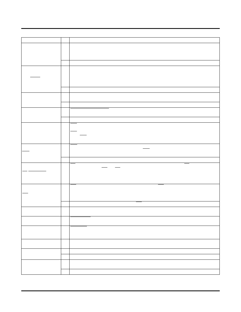
TDI, TCK, TMS
I
If boundary-scan is used, these pins are test data in, test clock, and test mode select inputs. If
boundary-scan is not selected, all boundary-scan functions are inhibited once conguration is
complete. Even if boundary-scan is not used, either TCK or TMS must be held at logic 1 during
conguration. Each pin has a pull-up enabled during conguration.
I/O After conguration, these pins are user-programmable I/O if boundary scan is not used.
1
RDY/BUSY/RCLK
O
During conguration in asynchronous peripheral mode, RDY/RCLK indicates another byte can
be written to the FPGA. If a read operation is done when the device is selected, the same sta-
tus is also available on D7 in asynchronous peripheral mode.
During the master parallel conguration mode, RCLK is a read output signal to an external
memory. This output is not normally used.
I/O After conguration this pin is a user-programmable I/O pin.
1
HDC
O
High During Conguration is output high until conguration is complete. It is used as a control
output, indicating that conguration is not complete.
I/O After conguration, this pin is a user-programmable I/O pin.
1
LDC
O
Low During Conguration
is output low until conguration is complete. It is used as a control out-
put, indicating that conguration is not complete.
I/O After conguration, this pin is a user-programmable I/O pin.
1
INIT
I/O INIT is a bidirectional signal before and during conguration. During conguration, a pull-up is
enabled, but an external pull-up resistor is recommended. As an active-low open-drain output,
INIT
is held low during power stabilization and internal clearing of memory. As an active-low
input, INIT holds the FPGA in the wait-state before the start of conguration.
After conguration, this pin is a user-programmable I/O pin.
1
CS0, CS1
I
CS0
and CS1 are used in the asynchronous peripheral, slave parallel, and microprocessor con-
guration modes. The FPGA is selected when CS0 is low and CS1 is high. During congura-
tion, a pull-up is enabled.
I/O After conguration, if MPI is not used, these pins are user-programmable I/O pins.
1
RD/MPI_STRB
I
RD
is used in the asynchronous peripheral conguration mode. A low on RD changes D[7:3]
into a status output. WR and RD should not be used simultaneously. If they are, the write strobe
overrides.
This pin is also used as the
MPI data transfer strobe. As a status indication, a high indicates
ready, and a low indicates busy.
WR/MPI_RW
I
WR is used in asynchronous peripheral mode. A low on WR transfers data on D[7:0] to the
FPGA.
In MPI mode, a high on MPI_RW allows a read from the data bus, while a low causes a write
transfer to the FPGA.
I/O After conguration, if the MPI is not used, WR/MPI_RW is a user-programmable I/O pin.
1
PPC_A[14:31]
I
During MPI mode the PPC_A[14:31] are used as the address bus driven by the PowerPC bus
master utilizing the least-signicant bits of the PowerPC 32-bit address.
MPI_BURST
I
MPI_BURST is driven low to indicate a burst transfer is in progress in MPI mode. Driven high
indicates that the current transfer is not a burst.
MPI_BDIP
I
MPI_BDIP is driven by the PowerPC processor in MPI mode. Assertion of this pin indicates that
the second beat in front of the current one is requested by the master. Negated before the burst
transfer ends to abort the burst data phase.
MPI_TSZ[0:1]
I
MPI_TSZ[0:1] signals are driven by the bus master in MPI mode to indicate the data transfer
size for the transaction. Set 01 for byte, 10 for half-word, and 00 for word.
A[21:0]
O
During master parallel mode A[21:0] address the conguration EPROMs up to 4M bytes.
I/O If not used for MPI these pins are user-programmable I/O pins after conguration.
1
MPI_ACK
O
In
MPI mode this is driven low indicating the MPI received the data on the write cycle or
returned data on a read cycle.
I/O If not used for MPI these pins are user-programmable I/O pins after conguration.
1
Table 40. Pin Descriptions (Continued)
Symbol
I/O
Description
相关PDF资料 |
PDF描述 |
|---|---|
| ORT82G5-2F680C | IC FPSC TRANSCEIVER 8CH 680-BGA |
| D38999/26JC8PN | CONN PLUG 8POS STRAIGHT W/PINS |
| MS27467T25F61SC | CONN PLUG 61POS STRAIGHT W/SCKT |
| 31-320-RFX | BNC PLUG, CRIMP RG-58 |
| D38999/24JD19PN | CONN RCPT 19POS JAM NUT W/PINS |
相关代理商/技术参数 |
参数描述 |
|---|---|
| ORT82G5-2FN680C | 功能描述:FPGA - 现场可编程门阵列 ORCA FPSC 1.5V 3.7 G b Bpln Xcvr 643K Gt RoHS:否 制造商:Altera Corporation 系列:Cyclone V E 栅极数量: 逻辑块数量:943 内嵌式块RAM - EBR:1956 kbit 输入/输出端数量:128 最大工作频率:800 MHz 工作电源电压:1.1 V 最大工作温度:+ 70 C 安装风格:SMD/SMT 封装 / 箱体:FBGA-256 |
| ORT82G5-2FN680C1 | 功能描述:FPGA - 现场可编程门阵列 10368 LUT 372 I/O RoHS:否 制造商:Altera Corporation 系列:Cyclone V E 栅极数量: 逻辑块数量:943 内嵌式块RAM - EBR:1956 kbit 输入/输出端数量:128 最大工作频率:800 MHz 工作电源电压:1.1 V 最大工作温度:+ 70 C 安装风格:SMD/SMT 封装 / 箱体:FBGA-256 |
| ORT82G5-2FN680I | 功能描述:FPGA - 现场可编程门阵列 ORCA FPSC 3.7 Gb Bp ln Xcvr 643K Gt I RoHS:否 制造商:Altera Corporation 系列:Cyclone V E 栅极数量: 逻辑块数量:943 内嵌式块RAM - EBR:1956 kbit 输入/输出端数量:128 最大工作频率:800 MHz 工作电源电压:1.1 V 最大工作温度:+ 70 C 安装风格:SMD/SMT 封装 / 箱体:FBGA-256 |
| ORT82G5-2FN680I1 | 功能描述:FPGA - 现场可编程门阵列 10368 LUT 372 I/O RoHS:否 制造商:Altera Corporation 系列:Cyclone V E 栅极数量: 逻辑块数量:943 内嵌式块RAM - EBR:1956 kbit 输入/输出端数量:128 最大工作频率:800 MHz 工作电源电压:1.1 V 最大工作温度:+ 70 C 安装风格:SMD/SMT 封装 / 箱体:FBGA-256 |
| ORT82G5-3BM680C | 功能描述:FPGA - 现场可编程门阵列 10368 LUT 372 I/O RoHS:否 制造商:Altera Corporation 系列:Cyclone V E 栅极数量: 逻辑块数量:943 内嵌式块RAM - EBR:1956 kbit 输入/输出端数量:128 最大工作频率:800 MHz 工作电源电压:1.1 V 最大工作温度:+ 70 C 安装风格:SMD/SMT 封装 / 箱体:FBGA-256 |
发布紧急采购,3分钟左右您将得到回复。