- 您现在的位置:买卖IC网 > PDF目录11731 > ORT82G5-2F680I (Lattice Semiconductor Corporation)IC FPSC TRANSCEIVER 8CH 680-BGA PDF资料下载
参数资料
| 型号: | ORT82G5-2F680I |
| 厂商: | Lattice Semiconductor Corporation |
| 文件页数: | 52/119页 |
| 文件大小: | 0K |
| 描述: | IC FPSC TRANSCEIVER 8CH 680-BGA |
| 产品变化通告: | Product Discontinuation 01/Aug/2011 |
| 标准包装: | 24 |
| 系列: | * |
第1页第2页第3页第4页第5页第6页第7页第8页第9页第10页第11页第12页第13页第14页第15页第16页第17页第18页第19页第20页第21页第22页第23页第24页第25页第26页第27页第28页第29页第30页第31页第32页第33页第34页第35页第36页第37页第38页第39页第40页第41页第42页第43页第44页第45页第46页第47页第48页第49页第50页第51页当前第52页第53页第54页第55页第56页第57页第58页第59页第60页第61页第62页第63页第64页第65页第66页第67页第68页第69页第70页第71页第72页第73页第74页第75页第76页第77页第78页第79页第80页第81页第82页第83页第84页第85页第86页第87页第88页第89页第90页第91页第92页第93页第94页第95页第96页第97页第98页第99页第100页第101页第102页第103页第104页第105页第106页第107页第108页第109页第110页第111页第112页第113页第114页第115页第116页第117页第118页第119页
Lattice Semiconductor
ORCA ORT42G5 and ORT82G5 Data Sheet
38
data rate and bit-width so the FPGA core can run at 1/4th this frequency which gives a range of 15 to 92.5 MHz for
the data in and out of the FPGA.
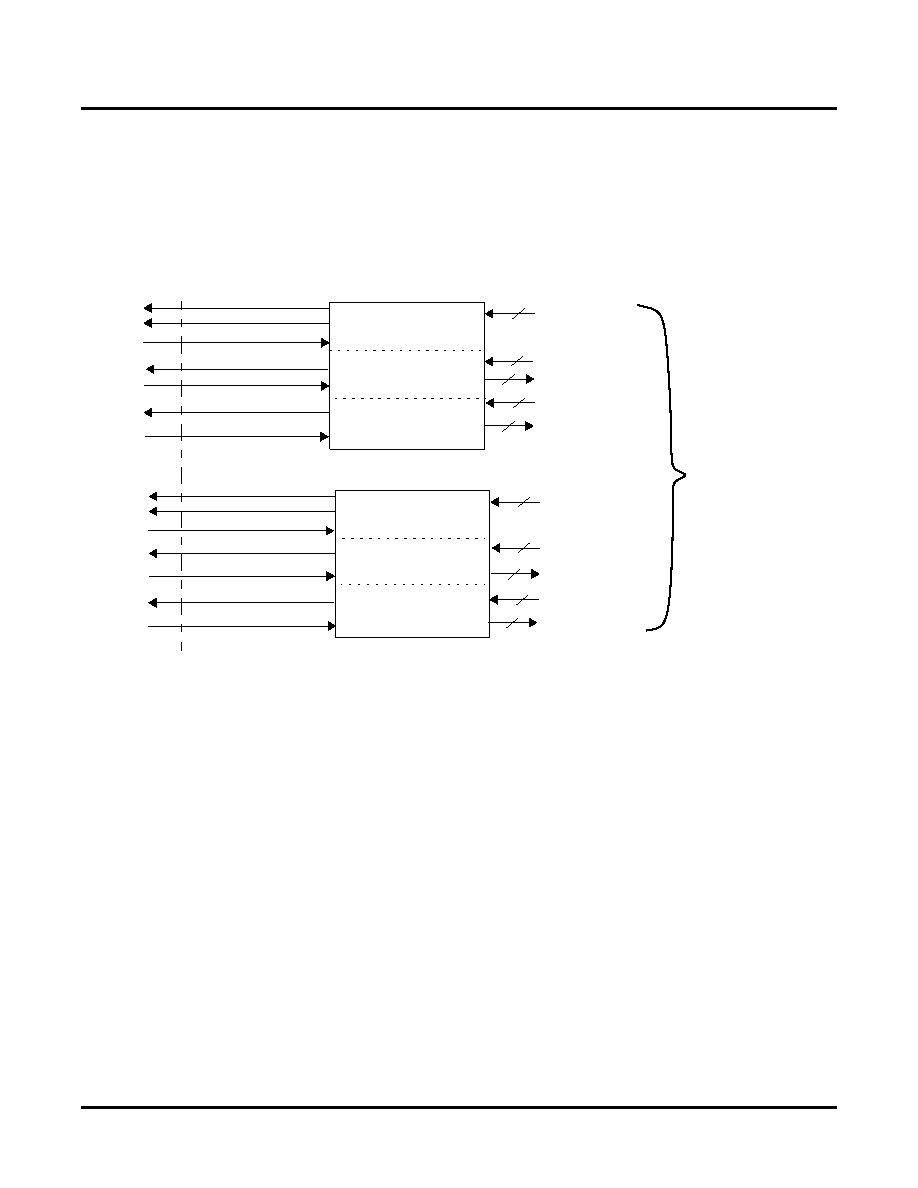
Internal Clock Signals at the FPGA/Core Interface for the ORT42G5
There are several clock signals dened at the FPGA/Embedded Core interface in addition to the external reference
clock for each SERDES block. All of the ORT42G5 clock signals are shown in Figure 17 and are described follow-
ing the gure.
Figure 17. ORT42G5 Clock Signals (High Speed Serial I/O Also Shown)
REFCLKP_[A:B], REFCLKN_[A:B]:
These are the differential reference clocks provided to the ORT42G5 device as described earlier. They are used as
the reference clock for both TX and RX paths. For operation of the serial links at 3.125 Gbps, the reference clocks
will be at a frequency of 156.25 MHz.
RWCK[AC, AD, BC, BD]:
These are the low-speed receive clocks from the embedded core to the FPGA across the core-FPGA interface.
These are derived from the recovered low-speed complementary clocks from the SERDES blocks. RWCKAC
belongs to Channel AC, RWCKBC belongs to channel BC and so on. With a reference clock input of 156.25 MHz,
these clocks operate at 78.125 MHz.
RCK78[A:B]:
These are muxed outputs of RWCKA[C or D] and RWCKB[C or D] respectively. With a reference clock input of
156.25 MHz, these clocks operate at 78.125 MHz.
RSYS_CLK_[A:B]2
These clocks are inputs to the SERDES blocks A and B respectively from the FPGA. These are used by each
channel as the read clock to read received data from the alignment FIFO within the embedded core. Clock
RSYS_CLK_A2 is used by channels in the SERDES block A and RSYS_CLK_B2 by channels in the SERDES
block B. To guarantee that there is no overow in the alignment FIFO, it is an absolute requirement that the write
and read clocks be frequency locked within 0 ppm. Examples of how to achieve this are shown in the later section
on recommended board-level clocking.
FPGA
Logic
Common Logic, Block A
Channel AC
Channel AD
RCK78A
TCK78A
RSYS_CLK_A2
TSYS_CLK_AC
RWCKAC
TSYS_CLK_AD
REFCLK[P:N]_A
2
HDIN[P:N]_AD
HDOUT[P:N]_AD
2
HDOUT[P:N]_AC
2
HDIN[P:N]_AC
2
TCK78A
Backplane
Serial
Link
Common Logic, Block B
Channel BC
Channel BD
RCK78B
TCK78B
RSYS_CLK_B2
TSYS_CLK_BC
RWCKBC
RWCKBD
TSYS_CLK_BD
REFCLK[P:N]_B
2
HDIN[P:N]_BD
HDOUT[P:N]_BD
2
HDOUT[P:N]_BC
2
HDIN[P:N]_BC
2
相关PDF资料 |
PDF描述 |
|---|---|
| ORT82G5-2F680C | IC FPSC TRANSCEIVER 8CH 680-BGA |
| D38999/26JC8PN | CONN PLUG 8POS STRAIGHT W/PINS |
| MS27467T25F61SC | CONN PLUG 61POS STRAIGHT W/SCKT |
| 31-320-RFX | BNC PLUG, CRIMP RG-58 |
| D38999/24JD19PN | CONN RCPT 19POS JAM NUT W/PINS |
相关代理商/技术参数 |
参数描述 |
|---|---|
| ORT82G5-2FN680C | 功能描述:FPGA - 现场可编程门阵列 ORCA FPSC 1.5V 3.7 G b Bpln Xcvr 643K Gt RoHS:否 制造商:Altera Corporation 系列:Cyclone V E 栅极数量: 逻辑块数量:943 内嵌式块RAM - EBR:1956 kbit 输入/输出端数量:128 最大工作频率:800 MHz 工作电源电压:1.1 V 最大工作温度:+ 70 C 安装风格:SMD/SMT 封装 / 箱体:FBGA-256 |
| ORT82G5-2FN680C1 | 功能描述:FPGA - 现场可编程门阵列 10368 LUT 372 I/O RoHS:否 制造商:Altera Corporation 系列:Cyclone V E 栅极数量: 逻辑块数量:943 内嵌式块RAM - EBR:1956 kbit 输入/输出端数量:128 最大工作频率:800 MHz 工作电源电压:1.1 V 最大工作温度:+ 70 C 安装风格:SMD/SMT 封装 / 箱体:FBGA-256 |
| ORT82G5-2FN680I | 功能描述:FPGA - 现场可编程门阵列 ORCA FPSC 3.7 Gb Bp ln Xcvr 643K Gt I RoHS:否 制造商:Altera Corporation 系列:Cyclone V E 栅极数量: 逻辑块数量:943 内嵌式块RAM - EBR:1956 kbit 输入/输出端数量:128 最大工作频率:800 MHz 工作电源电压:1.1 V 最大工作温度:+ 70 C 安装风格:SMD/SMT 封装 / 箱体:FBGA-256 |
| ORT82G5-2FN680I1 | 功能描述:FPGA - 现场可编程门阵列 10368 LUT 372 I/O RoHS:否 制造商:Altera Corporation 系列:Cyclone V E 栅极数量: 逻辑块数量:943 内嵌式块RAM - EBR:1956 kbit 输入/输出端数量:128 最大工作频率:800 MHz 工作电源电压:1.1 V 最大工作温度:+ 70 C 安装风格:SMD/SMT 封装 / 箱体:FBGA-256 |
| ORT82G5-3BM680C | 功能描述:FPGA - 现场可编程门阵列 10368 LUT 372 I/O RoHS:否 制造商:Altera Corporation 系列:Cyclone V E 栅极数量: 逻辑块数量:943 内嵌式块RAM - EBR:1956 kbit 输入/输出端数量:128 最大工作频率:800 MHz 工作电源电压:1.1 V 最大工作温度:+ 70 C 安装风格:SMD/SMT 封装 / 箱体:FBGA-256 |
发布紧急采购,3分钟左右您将得到回复。