- 您现在的位置:买卖IC网 > PDF目录11731 > ORT82G5-2F680I (Lattice Semiconductor Corporation)IC FPSC TRANSCEIVER 8CH 680-BGA PDF资料下载
参数资料
| 型号: | ORT82G5-2F680I |
| 厂商: | Lattice Semiconductor Corporation |
| 文件页数: | 68/119页 |
| 文件大小: | 0K |
| 描述: | IC FPSC TRANSCEIVER 8CH 680-BGA |
| 产品变化通告: | Product Discontinuation 01/Aug/2011 |
| 标准包装: | 24 |
| 系列: | * |
第1页第2页第3页第4页第5页第6页第7页第8页第9页第10页第11页第12页第13页第14页第15页第16页第17页第18页第19页第20页第21页第22页第23页第24页第25页第26页第27页第28页第29页第30页第31页第32页第33页第34页第35页第36页第37页第38页第39页第40页第41页第42页第43页第44页第45页第46页第47页第48页第49页第50页第51页第52页第53页第54页第55页第56页第57页第58页第59页第60页第61页第62页第63页第64页第65页第66页第67页当前第68页第69页第70页第71页第72页第73页第74页第75页第76页第77页第78页第79页第80页第81页第82页第83页第84页第85页第86页第87页第88页第89页第90页第91页第92页第93页第94页第95页第96页第97页第98页第99页第100页第101页第102页第103页第104页第105页第106页第107页第108页第109页第110页第111页第112页第113页第114页第115页第116页第117页第118页第119页
Lattice Semiconductor
ORCA ORT42G5 and ORT82G5 Data Sheet
52
Test Modes
In addition to the operational logic described in the preceding sections, the Embedded Core contains logic to sup-
port various test modes - both for device validation and evaluation and for operating system level tests. The follow-
ing sections discuss two of the test support logic blocks, supporting various loopback modes and SERDES
characterization.
Loopback Testing
Loopback testing is performed by looping back (either internal to the Embedded Core, by conguring the FPGA
logic or by external connections) transmitted data to the corresponding receiver inputs, or received data to the
transmitter output. The loopback path may be either serial or parallel.
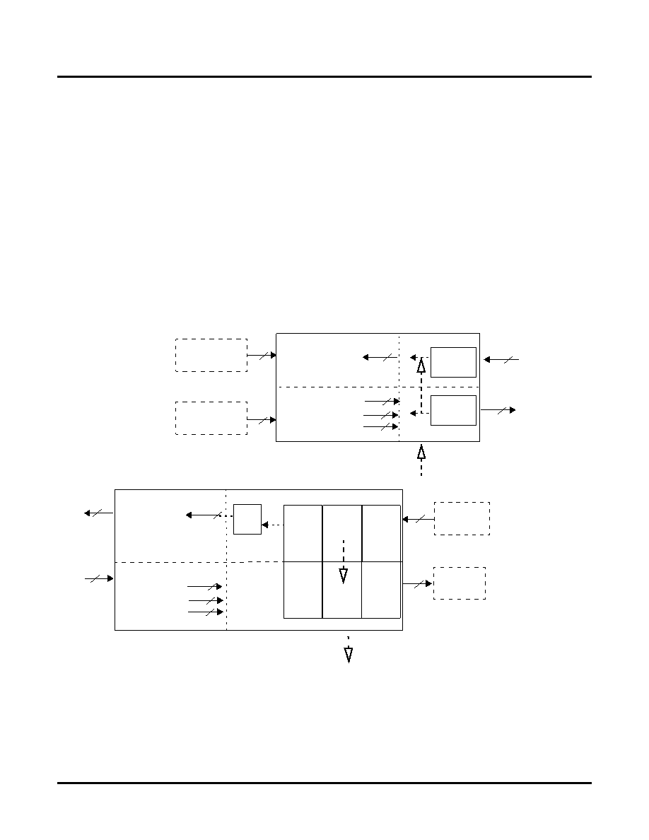
In general, loopback tests can be classied as “near end” or “far end.” In “near end” loopback (Figure 32(a)), data is
generated and checked locally, i.e. by logic on, or connection of, test equipment to the same card as the FPSC. In
“far end” loopback (Figure 32(b)), the generating and checking functions are performed remotely, either by test
equipment or a remote system card.
Figure 32. “Near End” vs. “Far End” Loopback
The loopback mode can also be characterized by the physical location of the loopback connection. There are three
possible loopback modes supported by the Embedded Core logic:
High-speed serial loopback at the CML buffer interface (near end)
Parallel loopback at the SERDES boundary (far end)
Device Under Test (DUT)
CML
Buffer
CML
Buffer
HDIN[P:N]_xx
2
Non-Functional
Embedded Core
FPGA Logic
40
MRWDxx[39:0]
32
4
Receive
Transmit
TWDxx[31:0]
TCOMMAxx[3:0]
TBIT9xx[3:0]
HDOUT[P:N]_xx
2
Data
Checking
Data
Generation
n
m
{
Active
(to Eye Diagram
Measurement or
remote System
Card)
Test Equipment
or Logic on Local
System Card
(a) “Near End” Loopback
High Speed
Serial Loopback
Connection
Device Under Test (DUT)
Data
Generation
Data
Checking
2
HDIN[P:N]_xx
HDOUT[P:N]_xx
{
n
m
Non-Functional
Active
(to Logic on
Local System
Card)
(b) “Far End” Loopback
FPGA Logic
40
MRWDxx[39:0]
Receive
4
Transmit
TWDxx[31:0]
TCOMMAxx[3:0]
TBIT9xx[3:0]
32
DE
MUX
8B/10B SERDES
CML
Buffer
8B/10B
CML
Buffer
SERDES Block
Parallel
Loopback
Connection
SERDES
Embedded Core
相关PDF资料 |
PDF描述 |
|---|---|
| ORT82G5-2F680C | IC FPSC TRANSCEIVER 8CH 680-BGA |
| D38999/26JC8PN | CONN PLUG 8POS STRAIGHT W/PINS |
| MS27467T25F61SC | CONN PLUG 61POS STRAIGHT W/SCKT |
| 31-320-RFX | BNC PLUG, CRIMP RG-58 |
| D38999/24JD19PN | CONN RCPT 19POS JAM NUT W/PINS |
相关代理商/技术参数 |
参数描述 |
|---|---|
| ORT82G5-2FN680C | 功能描述:FPGA - 现场可编程门阵列 ORCA FPSC 1.5V 3.7 G b Bpln Xcvr 643K Gt RoHS:否 制造商:Altera Corporation 系列:Cyclone V E 栅极数量: 逻辑块数量:943 内嵌式块RAM - EBR:1956 kbit 输入/输出端数量:128 最大工作频率:800 MHz 工作电源电压:1.1 V 最大工作温度:+ 70 C 安装风格:SMD/SMT 封装 / 箱体:FBGA-256 |
| ORT82G5-2FN680C1 | 功能描述:FPGA - 现场可编程门阵列 10368 LUT 372 I/O RoHS:否 制造商:Altera Corporation 系列:Cyclone V E 栅极数量: 逻辑块数量:943 内嵌式块RAM - EBR:1956 kbit 输入/输出端数量:128 最大工作频率:800 MHz 工作电源电压:1.1 V 最大工作温度:+ 70 C 安装风格:SMD/SMT 封装 / 箱体:FBGA-256 |
| ORT82G5-2FN680I | 功能描述:FPGA - 现场可编程门阵列 ORCA FPSC 3.7 Gb Bp ln Xcvr 643K Gt I RoHS:否 制造商:Altera Corporation 系列:Cyclone V E 栅极数量: 逻辑块数量:943 内嵌式块RAM - EBR:1956 kbit 输入/输出端数量:128 最大工作频率:800 MHz 工作电源电压:1.1 V 最大工作温度:+ 70 C 安装风格:SMD/SMT 封装 / 箱体:FBGA-256 |
| ORT82G5-2FN680I1 | 功能描述:FPGA - 现场可编程门阵列 10368 LUT 372 I/O RoHS:否 制造商:Altera Corporation 系列:Cyclone V E 栅极数量: 逻辑块数量:943 内嵌式块RAM - EBR:1956 kbit 输入/输出端数量:128 最大工作频率:800 MHz 工作电源电压:1.1 V 最大工作温度:+ 70 C 安装风格:SMD/SMT 封装 / 箱体:FBGA-256 |
| ORT82G5-3BM680C | 功能描述:FPGA - 现场可编程门阵列 10368 LUT 372 I/O RoHS:否 制造商:Altera Corporation 系列:Cyclone V E 栅极数量: 逻辑块数量:943 内嵌式块RAM - EBR:1956 kbit 输入/输出端数量:128 最大工作频率:800 MHz 工作电源电压:1.1 V 最大工作温度:+ 70 C 安装风格:SMD/SMT 封装 / 箱体:FBGA-256 |
发布紧急采购,3分钟左右您将得到回复。