- 您现在的位置:买卖IC网 > PDF目录11731 > ORT82G5-2F680I (Lattice Semiconductor Corporation)IC FPSC TRANSCEIVER 8CH 680-BGA PDF资料下载
参数资料
| 型号: | ORT82G5-2F680I |
| 厂商: | Lattice Semiconductor Corporation |
| 文件页数: | 59/119页 |
| 文件大小: | 0K |
| 描述: | IC FPSC TRANSCEIVER 8CH 680-BGA |
| 产品变化通告: | Product Discontinuation 01/Aug/2011 |
| 标准包装: | 24 |
| 系列: | * |
第1页第2页第3页第4页第5页第6页第7页第8页第9页第10页第11页第12页第13页第14页第15页第16页第17页第18页第19页第20页第21页第22页第23页第24页第25页第26页第27页第28页第29页第30页第31页第32页第33页第34页第35页第36页第37页第38页第39页第40页第41页第42页第43页第44页第45页第46页第47页第48页第49页第50页第51页第52页第53页第54页第55页第56页第57页第58页当前第59页第60页第61页第62页第63页第64页第65页第66页第67页第68页第69页第70页第71页第72页第73页第74页第75页第76页第77页第78页第79页第80页第81页第82页第83页第84页第85页第86页第87页第88页第89页第90页第91页第92页第93页第94页第95页第96页第97页第98页第99页第100页第101页第102页第103页第104页第105页第106页第107页第108页第109页第110页第111页第112页第113页第114页第115页第116页第117页第118页第119页
Lattice Semiconductor
ORCA ORT42G5 and ORT82G5 Data Sheet
44
RSYS_CLK_[A:B][1:2]
These clocks are inputs to the SERDES quad block A and B respectively from the FPGA. These are used by each
channel as the read clock to read received data from the alignment FIFO within the embedded core. Clocks
RSYS_CLK_A[1:2] are used by channels in the SERDES quad block A and RSYS_CLK_B[1:2] by channels in the
SERDES quad block B. To guarantee that there is no overow in the alignment FIFO, it is an absolute requirement
that the write and read clocks be frequency locked within 0 ppm. Examples of how to achieve this are shown in the
later section on recommended board-level clocking.
TCK78[A:B]:
This is a muxed output from the core to the FPGA across the core-FPGA interface of one of the 4 transmit SER-
DES clocks per quad operating at up to 92.5 MHz in the embedded core. There is one clock output per SERDES
quad block.
TSYS_CLK[AA,…BD]:
These clocks are inputs to the SERDES quad block A and B respectively from the FPGA. These are used by each
channel to control the timing of the Transmit Data Path. To guarantee correct transmit operation theses clocks must
be frequency locked within 0 ppm to TCK78[A:B].
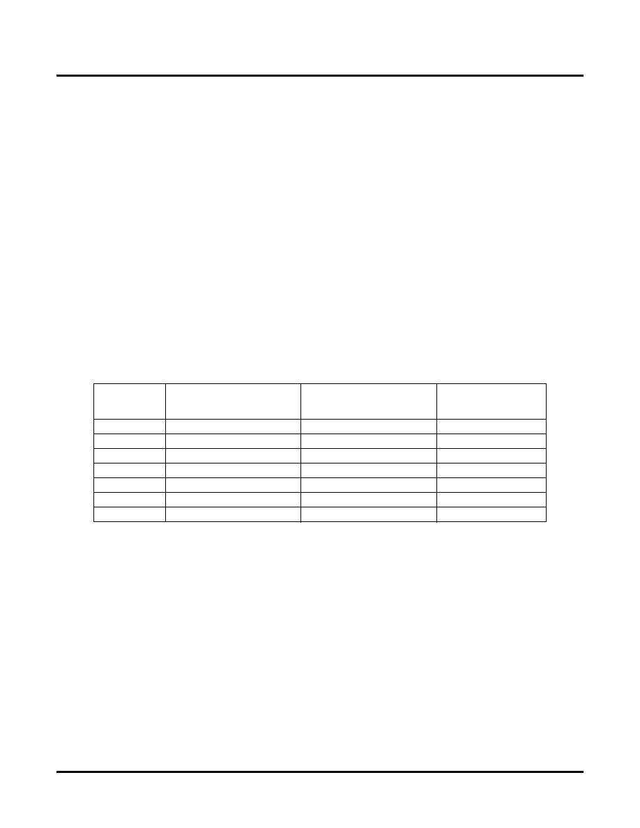
Transmit and Receive Clock Rates
Table 16 shows the typical relationship between the data rates, the reference clock, the transmit TCK78[A:B] clock
and the receive RCK78[A:B] clock. The selection of full-rate or half-rate for a given reference clock speed is set by
bits in the transmit and receive control registers and can be set per channel.
Table 16. Transmit Data and Clock Rates
Besides taking in a TSYS_CLK_xx from the FPGA logic for each channel, the transmit path logic sends back a
clock of the same frequency, but arbitrary phase. This clock, TCK78[A:B], is derived from the MUX block of one of
the 4 channels in its SERDES quad. The MUX blocks provide the potential source for TCK78[A:B] by a divide-by-4
of the SERDES STBC311xs clock used in synchronizing the transmit data words in the STBC311xx clock domain.
The STBC311xx clocks are internal to the core and are not brought across the core/FPGA interface.
The receiver section receives high-speed serial data at its differential CML input port and sends in to the Clock and
Data Recovery (CDR) block. The CDR block then generates a recovered clock (RWCKxx) and retimes the data.
Thus, the recovered receive clocks are asynchronous between channels.
Transmit Clock Source Selection
The TCKSEL[0:1][A:B] bits select the source channel of TCK78[A:B]. The selection of the source for TCK78[A:B] is
controlled by these bits as shown in Table 17.
Data Rate
Reference Clock
TCK78[A: B] and RCK78[A:B]
Clocks
Rate of Channel
Selected as Clock
Source
0.6 Gbps
60 MHz
15 MHz
Half
1.0 Gbps
100 MHz
25 MHz
Half
1.25 Gbps
125 MHz
31.25 MHz
Half
2.0 Gbps
100 MHz
50 MHz
Full
2.5 Gbps
125 MHz
62.5 MHz
Full
3.125 Gbps
156 MHz
78 MHz
Full
3.7 Gbps
185 MHz
92.5 MHz
Full
相关PDF资料 |
PDF描述 |
|---|---|
| ORT82G5-2F680C | IC FPSC TRANSCEIVER 8CH 680-BGA |
| D38999/26JC8PN | CONN PLUG 8POS STRAIGHT W/PINS |
| MS27467T25F61SC | CONN PLUG 61POS STRAIGHT W/SCKT |
| 31-320-RFX | BNC PLUG, CRIMP RG-58 |
| D38999/24JD19PN | CONN RCPT 19POS JAM NUT W/PINS |
相关代理商/技术参数 |
参数描述 |
|---|---|
| ORT82G5-2FN680C | 功能描述:FPGA - 现场可编程门阵列 ORCA FPSC 1.5V 3.7 G b Bpln Xcvr 643K Gt RoHS:否 制造商:Altera Corporation 系列:Cyclone V E 栅极数量: 逻辑块数量:943 内嵌式块RAM - EBR:1956 kbit 输入/输出端数量:128 最大工作频率:800 MHz 工作电源电压:1.1 V 最大工作温度:+ 70 C 安装风格:SMD/SMT 封装 / 箱体:FBGA-256 |
| ORT82G5-2FN680C1 | 功能描述:FPGA - 现场可编程门阵列 10368 LUT 372 I/O RoHS:否 制造商:Altera Corporation 系列:Cyclone V E 栅极数量: 逻辑块数量:943 内嵌式块RAM - EBR:1956 kbit 输入/输出端数量:128 最大工作频率:800 MHz 工作电源电压:1.1 V 最大工作温度:+ 70 C 安装风格:SMD/SMT 封装 / 箱体:FBGA-256 |
| ORT82G5-2FN680I | 功能描述:FPGA - 现场可编程门阵列 ORCA FPSC 3.7 Gb Bp ln Xcvr 643K Gt I RoHS:否 制造商:Altera Corporation 系列:Cyclone V E 栅极数量: 逻辑块数量:943 内嵌式块RAM - EBR:1956 kbit 输入/输出端数量:128 最大工作频率:800 MHz 工作电源电压:1.1 V 最大工作温度:+ 70 C 安装风格:SMD/SMT 封装 / 箱体:FBGA-256 |
| ORT82G5-2FN680I1 | 功能描述:FPGA - 现场可编程门阵列 10368 LUT 372 I/O RoHS:否 制造商:Altera Corporation 系列:Cyclone V E 栅极数量: 逻辑块数量:943 内嵌式块RAM - EBR:1956 kbit 输入/输出端数量:128 最大工作频率:800 MHz 工作电源电压:1.1 V 最大工作温度:+ 70 C 安装风格:SMD/SMT 封装 / 箱体:FBGA-256 |
| ORT82G5-3BM680C | 功能描述:FPGA - 现场可编程门阵列 10368 LUT 372 I/O RoHS:否 制造商:Altera Corporation 系列:Cyclone V E 栅极数量: 逻辑块数量:943 内嵌式块RAM - EBR:1956 kbit 输入/输出端数量:128 最大工作频率:800 MHz 工作电源电压:1.1 V 最大工作温度:+ 70 C 安装风格:SMD/SMT 封装 / 箱体:FBGA-256 |
发布紧急采购,3分钟左右您将得到回复。