- 您现在的位置:买卖IC网 > PDF目录11731 > ORT82G5-2F680I (Lattice Semiconductor Corporation)IC FPSC TRANSCEIVER 8CH 680-BGA PDF资料下载
参数资料
| 型号: | ORT82G5-2F680I |
| 厂商: | Lattice Semiconductor Corporation |
| 文件页数: | 96/119页 |
| 文件大小: | 0K |
| 描述: | IC FPSC TRANSCEIVER 8CH 680-BGA |
| 产品变化通告: | Product Discontinuation 01/Aug/2011 |
| 标准包装: | 24 |
| 系列: | * |
第1页第2页第3页第4页第5页第6页第7页第8页第9页第10页第11页第12页第13页第14页第15页第16页第17页第18页第19页第20页第21页第22页第23页第24页第25页第26页第27页第28页第29页第30页第31页第32页第33页第34页第35页第36页第37页第38页第39页第40页第41页第42页第43页第44页第45页第46页第47页第48页第49页第50页第51页第52页第53页第54页第55页第56页第57页第58页第59页第60页第61页第62页第63页第64页第65页第66页第67页第68页第69页第70页第71页第72页第73页第74页第75页第76页第77页第78页第79页第80页第81页第82页第83页第84页第85页第86页第87页第88页第89页第90页第91页第92页第93页第94页第95页当前第96页第97页第98页第99页第100页第101页第102页第103页第104页第105页第106页第107页第108页第109页第110页第111页第112页第113页第114页第115页第116页第117页第118页第119页
Lattice Semiconductor
ORCA ORT42G5 and ORT82G5 Data Sheet
78
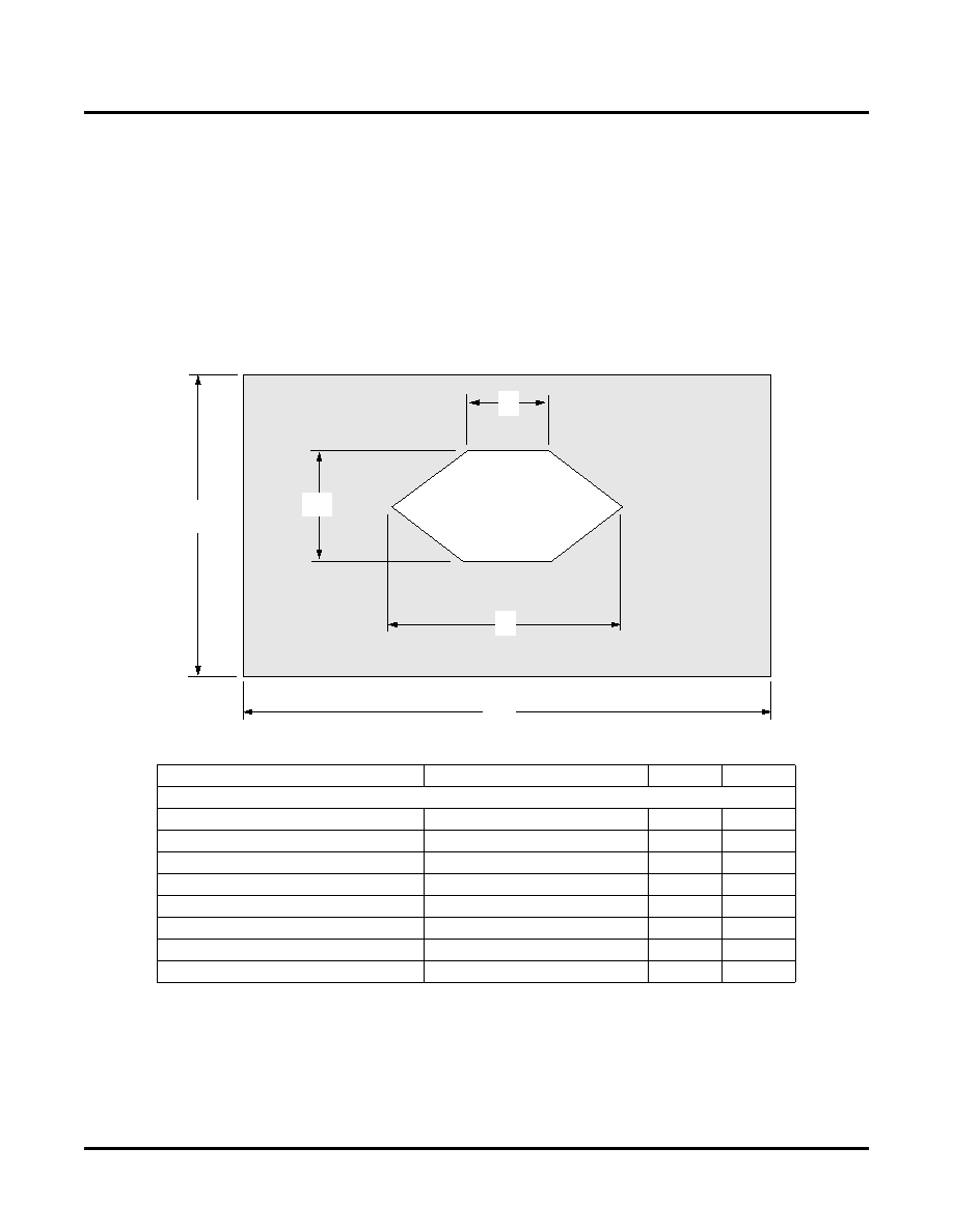
Input Eye-Mask Characterization
Figure 39. provides an eye-mask characterization of the SERDES receiver input. The eye-mask is specied below
for two different eye-mask heights. It provides guidance on a number of input parameters, including signal ampli-
tude and rise time limits, noise and jitter limits, and P and N input skew tolerance. Almost all detrimental character-
istics of transmit signal and the interconnection link design result in eye-closure. This, combined with the eye-
opening limitations of the line receiver, can provide a good indication of a link’s ability to transfer data error-free.
The Clock and Data Recovery (CDR) portion of the ORT42G5 and ORT82G5 SERDES receiver has the ability to
lter incoming signal jitter that is below the clock recovery PLL bandwidth (about 3 MHz). The eye-mask specica-
tions of Table 37 are for jitter frequencies above the PLL bandwidth of the CDR, which is a worst case condition.
When jitter occurs at frequencies below the PLL bandwidth, the receiver jitter tolerance is signicantly better. For
this case error-free data detection can occur even with a completely closed eye-mask.
Figure 39. Receive Data Eye-Diagram Template (Differential)
Table 37. Receiver Eye-Mask Specications1
Parameter
Conditions
Value
Unit
Input Data
Eye Opening Width (H)@ 3.125Gbps
V=175 mV diff
1
0.55
UIP-P
Eye Opening Width (T)@ 3.125Gbps
V=175 mV diff
1
0.15
UIP-P
Eye Opening Width (H)@ 3.125Gbps
V=600 mV diff
1
0.35
UIP-P
Eye Opening Width (T)@ 3.125Gbps
V=600 mV diff
1
0.10
UIP-P
Eye Opening Width (H)@ 2.5Gbps
V=175 mV diff
1
0.42
UIP-P
Eye Opening Width (T)@ 2.5Gbps
V=175 mV diff
1
0.15
UIP-P
Eye Opening Width (H)@ 2.5Gbps
V=600 mV diff
1
0.33
UIP-P
Eye Opening Width (T)@ 2.5Gbps
V=600 mV diff
1
0.10
UIP-P
1. With PRBS 2^7-1 data pattern, 10 MHz sinusoidal jitter, all channels operating, FPGA logic active, REFCLK jitter
of 30 ps., TA = 0
oC to 85oC, 1.425V to 1.575V supply.
H
V
1.2V
UI
T
相关PDF资料 |
PDF描述 |
|---|---|
| ORT82G5-2F680C | IC FPSC TRANSCEIVER 8CH 680-BGA |
| D38999/26JC8PN | CONN PLUG 8POS STRAIGHT W/PINS |
| MS27467T25F61SC | CONN PLUG 61POS STRAIGHT W/SCKT |
| 31-320-RFX | BNC PLUG, CRIMP RG-58 |
| D38999/24JD19PN | CONN RCPT 19POS JAM NUT W/PINS |
相关代理商/技术参数 |
参数描述 |
|---|---|
| ORT82G5-2FN680C | 功能描述:FPGA - 现场可编程门阵列 ORCA FPSC 1.5V 3.7 G b Bpln Xcvr 643K Gt RoHS:否 制造商:Altera Corporation 系列:Cyclone V E 栅极数量: 逻辑块数量:943 内嵌式块RAM - EBR:1956 kbit 输入/输出端数量:128 最大工作频率:800 MHz 工作电源电压:1.1 V 最大工作温度:+ 70 C 安装风格:SMD/SMT 封装 / 箱体:FBGA-256 |
| ORT82G5-2FN680C1 | 功能描述:FPGA - 现场可编程门阵列 10368 LUT 372 I/O RoHS:否 制造商:Altera Corporation 系列:Cyclone V E 栅极数量: 逻辑块数量:943 内嵌式块RAM - EBR:1956 kbit 输入/输出端数量:128 最大工作频率:800 MHz 工作电源电压:1.1 V 最大工作温度:+ 70 C 安装风格:SMD/SMT 封装 / 箱体:FBGA-256 |
| ORT82G5-2FN680I | 功能描述:FPGA - 现场可编程门阵列 ORCA FPSC 3.7 Gb Bp ln Xcvr 643K Gt I RoHS:否 制造商:Altera Corporation 系列:Cyclone V E 栅极数量: 逻辑块数量:943 内嵌式块RAM - EBR:1956 kbit 输入/输出端数量:128 最大工作频率:800 MHz 工作电源电压:1.1 V 最大工作温度:+ 70 C 安装风格:SMD/SMT 封装 / 箱体:FBGA-256 |
| ORT82G5-2FN680I1 | 功能描述:FPGA - 现场可编程门阵列 10368 LUT 372 I/O RoHS:否 制造商:Altera Corporation 系列:Cyclone V E 栅极数量: 逻辑块数量:943 内嵌式块RAM - EBR:1956 kbit 输入/输出端数量:128 最大工作频率:800 MHz 工作电源电压:1.1 V 最大工作温度:+ 70 C 安装风格:SMD/SMT 封装 / 箱体:FBGA-256 |
| ORT82G5-3BM680C | 功能描述:FPGA - 现场可编程门阵列 10368 LUT 372 I/O RoHS:否 制造商:Altera Corporation 系列:Cyclone V E 栅极数量: 逻辑块数量:943 内嵌式块RAM - EBR:1956 kbit 输入/输出端数量:128 最大工作频率:800 MHz 工作电源电压:1.1 V 最大工作温度:+ 70 C 安装风格:SMD/SMT 封装 / 箱体:FBGA-256 |
发布紧急采购,3分钟左右您将得到回复。