- 您现在的位置:买卖IC网 > PDF目录11731 > ORT82G5-2F680I (Lattice Semiconductor Corporation)IC FPSC TRANSCEIVER 8CH 680-BGA PDF资料下载
参数资料
| 型号: | ORT82G5-2F680I |
| 厂商: | Lattice Semiconductor Corporation |
| 文件页数: | 72/119页 |
| 文件大小: | 0K |
| 描述: | IC FPSC TRANSCEIVER 8CH 680-BGA |
| 产品变化通告: | Product Discontinuation 01/Aug/2011 |
| 标准包装: | 24 |
| 系列: | * |
第1页第2页第3页第4页第5页第6页第7页第8页第9页第10页第11页第12页第13页第14页第15页第16页第17页第18页第19页第20页第21页第22页第23页第24页第25页第26页第27页第28页第29页第30页第31页第32页第33页第34页第35页第36页第37页第38页第39页第40页第41页第42页第43页第44页第45页第46页第47页第48页第49页第50页第51页第52页第53页第54页第55页第56页第57页第58页第59页第60页第61页第62页第63页第64页第65页第66页第67页第68页第69页第70页第71页当前第72页第73页第74页第75页第76页第77页第78页第79页第80页第81页第82页第83页第84页第85页第86页第87页第88页第89页第90页第91页第92页第93页第94页第95页第96页第97页第98页第99页第100页第101页第102页第103页第104页第105页第106页第107页第108页第109页第110页第111页第112页第113页第114页第115页第116页第117页第118页第119页
Lattice Semiconductor
ORCA ORT42G5 and ORT82G5 Data Sheet
56
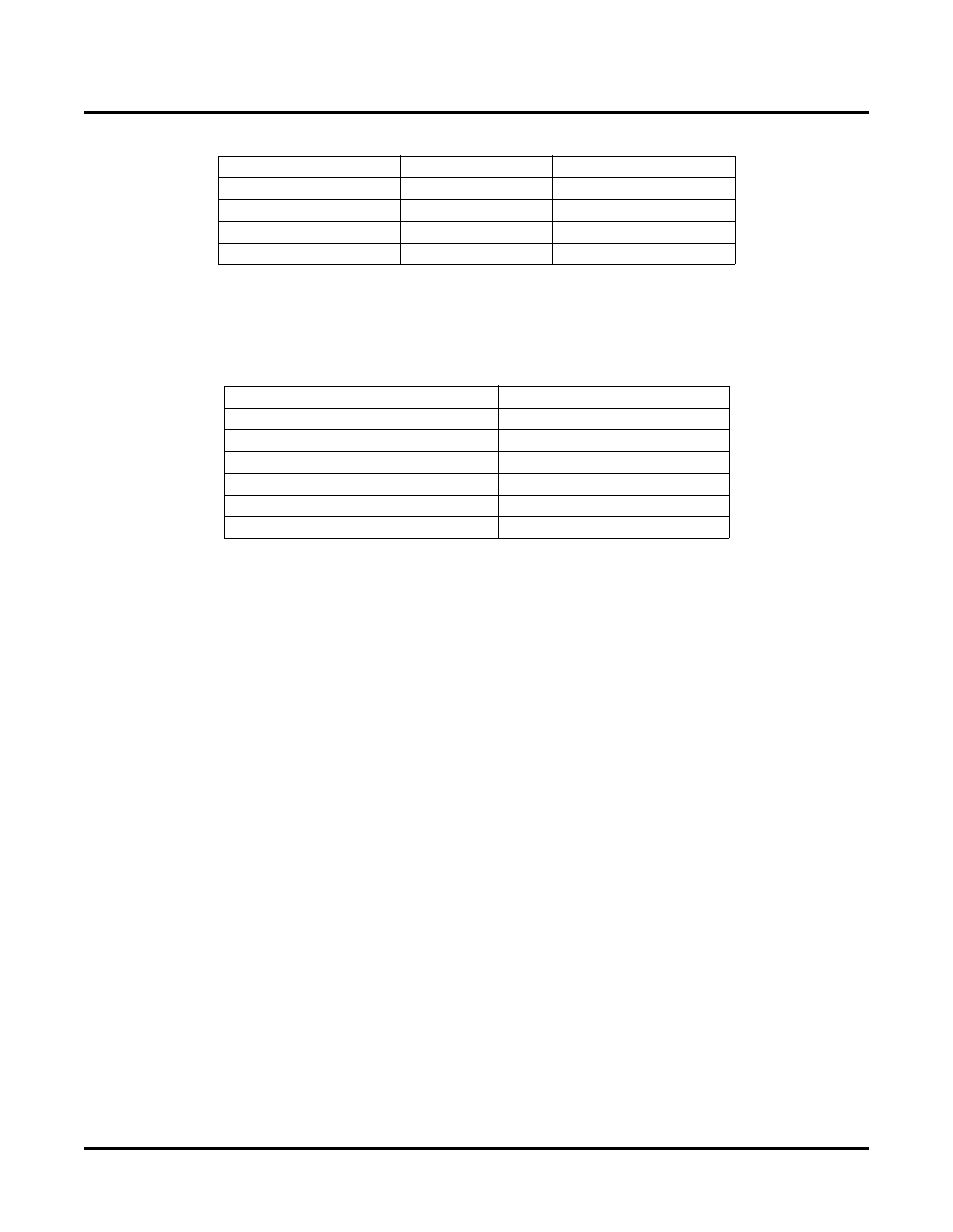
Table 24. Decoding of SCHAR_CHAN
The receive characterization test mode is entered when SCHAR_ENA=1 and SCHAR_TXSEL=0, In this mode,
one of the channels of SERDES outputs is observed at chip ports as shown in Table 25. The channel that is
observed is also based on the decoding of SCHAR_CHAN as shown in Table 25.
Table 25. SERDES Receive Characterization Mode
Embedded Core Block RAM
There are two independent memory blocks (labeled A and B) built-into the Embedded ASIC Core (EAC). Each
memory block has a capacity of 4K words by 36 bits. These two memory blocks (also called “slices”) are in addition
to the block RAMs found in the FPGA portion of the ORT82G5.
Although the memory blocks/slices are in the EAC part of the chip, they do not interact with the rest of the EAC cir-
cuits, but are standalone memories designed specically to increase RAM capacity in the ORT82G5 chip. They can
be used by logic implemented in the FPGA portion of the FPSC. Figure 34 represents one of the two available
memory slices built into the EAC. The index “x” refers to the memory slice (x=A for slice A, x=B for slice B). Each
memory slice is organized into two sections, which are also labeled as A and B. In Figure 34, SDRAM A is one sec-
tion of slice x, and SDRAM B is another section of slice x. Data can be written to both sections of a slice indepen-
dently. However, a read access can access only one of sections A or B at any given time (CSR_x=0 selects section
A, CSR_x=1 selects section B).
The 36 bits written to or read from the memory slice are composed of 32 bits of data (bits 31:24, 23:16, 15:8, 7:0),
and 4 bits of parity (bits 35,34,33,32). The core performs no parity checking functions. The data read from the
memory is registered so that it works as a pipelined synchronous memory block.
For illustration purposes, assuming that the memory slice in Figure 34 is slice A (x=A), then certain signals apply to
both sections of slice A. These include D_A[35:0], CKW_A, AW_A[10:0], BYTEWN_A[3:0], Q_A[35:0], CKR_A,
CSR_A, and AR_A[10:0]. The BYTEWN_A[3:0] are byte and parity write enable bits for each byte and parity bit of
data being written.
BYTEWN_A[3] is associated with D_A[35,31:24].
BYTEWN_A[2] is associated with D_A[34,23:16].
BYTEWN_A[1] is associated with D_A[33,15:8].
BYTEWN_A[0] is associated with D_A[32,7:0].
The signals that are unique to each section of slice A are:
CSWA_A --enables writing to section A of slice A
CSWB_A -- enables writing to section B of slice A
SCHAR_CHAN0
SCHAR_CHAN1
Channel
0
BA
1
0
BB
0
1
BC
1
BD
SERDES Output
Chip Port
BYTSYNCBx
PSCHAR_BYTSYNC
WDSYNCBx
PSCHAR_WDSYNC
CVOBx
PSCHAR_CV
LDOUTBx[9:0]
PSCHAR_LDIO[9:0]
RBC0Bx
PSCHAR_CKIO0
RBC1Bx
PSCHAR_CKIO1
相关PDF资料 |
PDF描述 |
|---|---|
| ORT82G5-2F680C | IC FPSC TRANSCEIVER 8CH 680-BGA |
| D38999/26JC8PN | CONN PLUG 8POS STRAIGHT W/PINS |
| MS27467T25F61SC | CONN PLUG 61POS STRAIGHT W/SCKT |
| 31-320-RFX | BNC PLUG, CRIMP RG-58 |
| D38999/24JD19PN | CONN RCPT 19POS JAM NUT W/PINS |
相关代理商/技术参数 |
参数描述 |
|---|---|
| ORT82G5-2FN680C | 功能描述:FPGA - 现场可编程门阵列 ORCA FPSC 1.5V 3.7 G b Bpln Xcvr 643K Gt RoHS:否 制造商:Altera Corporation 系列:Cyclone V E 栅极数量: 逻辑块数量:943 内嵌式块RAM - EBR:1956 kbit 输入/输出端数量:128 最大工作频率:800 MHz 工作电源电压:1.1 V 最大工作温度:+ 70 C 安装风格:SMD/SMT 封装 / 箱体:FBGA-256 |
| ORT82G5-2FN680C1 | 功能描述:FPGA - 现场可编程门阵列 10368 LUT 372 I/O RoHS:否 制造商:Altera Corporation 系列:Cyclone V E 栅极数量: 逻辑块数量:943 内嵌式块RAM - EBR:1956 kbit 输入/输出端数量:128 最大工作频率:800 MHz 工作电源电压:1.1 V 最大工作温度:+ 70 C 安装风格:SMD/SMT 封装 / 箱体:FBGA-256 |
| ORT82G5-2FN680I | 功能描述:FPGA - 现场可编程门阵列 ORCA FPSC 3.7 Gb Bp ln Xcvr 643K Gt I RoHS:否 制造商:Altera Corporation 系列:Cyclone V E 栅极数量: 逻辑块数量:943 内嵌式块RAM - EBR:1956 kbit 输入/输出端数量:128 最大工作频率:800 MHz 工作电源电压:1.1 V 最大工作温度:+ 70 C 安装风格:SMD/SMT 封装 / 箱体:FBGA-256 |
| ORT82G5-2FN680I1 | 功能描述:FPGA - 现场可编程门阵列 10368 LUT 372 I/O RoHS:否 制造商:Altera Corporation 系列:Cyclone V E 栅极数量: 逻辑块数量:943 内嵌式块RAM - EBR:1956 kbit 输入/输出端数量:128 最大工作频率:800 MHz 工作电源电压:1.1 V 最大工作温度:+ 70 C 安装风格:SMD/SMT 封装 / 箱体:FBGA-256 |
| ORT82G5-3BM680C | 功能描述:FPGA - 现场可编程门阵列 10368 LUT 372 I/O RoHS:否 制造商:Altera Corporation 系列:Cyclone V E 栅极数量: 逻辑块数量:943 内嵌式块RAM - EBR:1956 kbit 输入/输出端数量:128 最大工作频率:800 MHz 工作电源电压:1.1 V 最大工作温度:+ 70 C 安装风格:SMD/SMT 封装 / 箱体:FBGA-256 |
发布紧急采购,3分钟左右您将得到回复。