参数资料
| 型号: | PIC12F1822-I/MF |
| 厂商: | Microchip Technology |
| 文件页数: | 62/109页 |
| 文件大小: | 0K |
| 描述: | IC MCU 8BIT FLASH 8DFN |
| 产品培训模块: | 8-bit PIC® Microcontroller Portfolio |
| 标准包装: | 120 |
| 系列: | PIC® XLP™ 12F |
| 核心处理器: | PIC |
| 芯体尺寸: | 8-位 |
| 速度: | 32MHz |
| 连通性: | I²C,LIN,SPI,UART/USART |
| 外围设备: | 欠压检测/复位,POR,PWM,WDT |
| 输入/输出数: | 6 |
| 程序存储器容量: | 3.5KB(2K x 14) |
| 程序存储器类型: | 闪存 |
| EEPROM 大小: | 256 x 8 |
| RAM 容量: | 128 x 8 |
| 电压 - 电源 (Vcc/Vdd): | 1.8 V ~ 5.5 V |
| 数据转换器: | A/D 4x10b |
| 振荡器型: | 内部 |
| 工作温度: | -40°C ~ 85°C |
| 封装/外壳: | 8-VDFN 裸露焊盘 |
| 包装: | 管件 |
第1页第2页第3页第4页第5页第6页第7页第8页第9页第10页第11页第12页第13页第14页第15页第16页第17页第18页第19页第20页第21页第22页第23页第24页第25页第26页第27页第28页第29页第30页第31页第32页第33页第34页第35页第36页第37页第38页第39页第40页第41页第42页第43页第44页第45页第46页第47页第48页第49页第50页第51页第52页第53页第54页第55页第56页第57页第58页第59页第60页第61页当前第62页第63页第64页第65页第66页第67页第68页第69页第70页第71页第72页第73页第74页第75页第76页第77页第78页第79页第80页第81页第82页第83页第84页第85页第86页第87页第88页第89页第90页第91页第92页第93页第94页第95页第96页第97页第98页第99页第100页第101页第102页第103页第104页第105页第106页第107页第108页第109页
247
7674F–AVR–09/09
ATmega164P/324P/644P
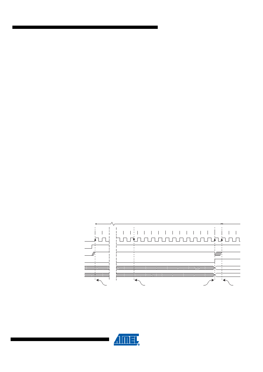
in ADCSRA. The prescaler keeps running for as long as the ADEN bit is set, and is continuously
reset when ADEN is low.
When initiating a single ended conversion by setting the ADSC bit in ADCSRA, the conversion
starts at the following rising edge of the ADC clock cycle. See “Differential Gain Channels” on
page 249 for details on differential conversion timing.
A normal conversion takes 13 ADC clock cycles. The first conversion after the ADC is switched
on (ADEN in ADCSRA is set) takes 25 ADC clock cycles in order to initialize the analog circuitry.
When the bandgap reference voltage is used as input to the ADC, it will take a certain time for
the voltage to stabilize. If not stabilized, the first value read after the first conversion may be
wrong.
The actual sample-and-hold takes place 1.5 ADC clock cycles after the start of a normal conver-
sion and 13.5 ADC clock cycles after the start of a first conversion. When a conversion is
complete, the result is written to the ADC Data Registers, and ADIF is set. In single conversion
mode, ADSC is cleared simultaneously. The software may then set ADSC again, and a new
conversion will be initiated on the first rising ADC clock edge.
When Auto Triggering is used, the prescaler is reset when the trigger event occurs. This assures
a fixed delay from the trigger event to the start of conversion. In this mode, the sample-and-hold
takes place 2 ADC clock cycles after the rising edge on the trigger source signal. Three addi-
tional CPU clock cycles are used for synchronization logic.
When using Differential mode, along with Auto Trigging from a source other than the ADC Con-
version Complete, each conversion will require 25 ADC clocks. This is because the ADC must
be disabled and re-enabled after every conversion.
In Free Running mode, a new conversion will be started immediately after the conversion com-
pletes, while ADSC remains high. For a summary of conversion times, see Table 21-1 on page
Figure 21-4. ADC Timing Diagram, First Conversion (Single Conversion Mode)
MSB of Result
LSB of Result
ADC Clock
ADSC
Sample & Hold
ADIF
ADCH
ADCL
Cycle Number
ADEN
1
212
13
14
15
16
17
18
19
20
21
22
23
24
25
1
2
First Conversion
Next
Conversion
3
MUX and REFS
Update
MUX and REFS
Update
Conversion
Complete
相关PDF资料 |
PDF描述 |
|---|---|
| PIC18LC452T-I/L | IC MCU OTP 16KX16 A/D 44PLCC |
| PIC17LC43T-08I/L | IC MCU OTP 4KX16 PWM 44PLCC |
| PIC12F629-I/P | IC MCU CMOS FLASH-BASE 8BIT 8DIP |
| PIC12F675-I/SN | IC MCU CMOS FLSH-BASE 8BIT 8SOIC |
| PIC17LC43T-08/PT | IC MCU OTP 4KX16 PWM 44TQFP |
相关代理商/技术参数 |
参数描述 |
|---|---|
| PIC12F1822T-E/SN | 制造商:Microchip Technology Inc 功能描述:PIC12F Series 128 B RAM 3.5 kB Flash 8-Bit CMOS Microcontroller - SOIC-8 |
| PIC12F1822T-I/MF | 功能描述:8位微控制器 -MCU 3.5KB 128B RAM 32MHz RoHS:否 制造商:Silicon Labs 核心:8051 处理器系列:C8051F39x 数据总线宽度:8 bit 最大时钟频率:50 MHz 程序存储器大小:16 KB 数据 RAM 大小:1 KB 片上 ADC:Yes 工作电源电压:1.8 V to 3.6 V 工作温度范围:- 40 C to + 105 C 封装 / 箱体:QFN-20 安装风格:SMD/SMT |
| PIC12F1822T-I/SN | 功能描述:8位微控制器 -MCU 3.5KB 128B RAM 32MHz Int. Osc 6 I/0 RoHS:否 制造商:Silicon Labs 核心:8051 处理器系列:C8051F39x 数据总线宽度:8 bit 最大时钟频率:50 MHz 程序存储器大小:16 KB 数据 RAM 大小:1 KB 片上 ADC:Yes 工作电源电压:1.8 V to 3.6 V 工作温度范围:- 40 C to + 105 C 封装 / 箱体:QFN-20 安装风格:SMD/SMT |
| PIC12F1822T-I/SS | 制造商:MICROCHIP 制造商全称:Microchip Technology 功能描述:8/14-Pin Flash Microcontrollers with nanoWatt XLP Technology |
| PIC12F1840 | 制造商:MICROCHIP 制造商全称:Microchip Technology 功能描述:8-Pin Flash Microcontrollers with nanoWatt XLP Technology |
发布紧急采购,3分钟左右您将得到回复。