- 您现在的位置:买卖IC网 > PDF目录268241 > PIC17CXX (Microchip Technology Inc.) EPROM Memory Programming Specification PDF资料下载
参数资料
| 型号: | PIC17CXX |
| 厂商: | Microchip Technology Inc. |
| 英文描述: | EPROM Memory Programming Specification |
| 中文描述: | EPROM存储器编程规范 |
| 文件页数: | 19/71页 |
| 文件大小: | 1173K |
| 代理商: | PIC17CXX |
第1页第2页第3页第4页第5页第6页第7页第8页第9页第10页第11页第12页第13页第14页第15页第16页第17页第18页当前第19页第20页第21页第22页第23页第24页第25页第26页第27页第28页第29页第30页第31页第32页第33页第34页第35页第36页第37页第38页第39页第40页第41页第42页第43页第44页第45页第46页第47页第48页第49页第50页第51页第52页第53页第54页第55页第56页第57页第58页第59页第60页第61页第62页第63页第64页第65页第66页第67页第68页第69页第70页第71页
PIC17C4X
DS30412C-page 26
1996 Microchip Technology Inc.
5.5
RA0/INT Interrupt
The external interrupt on the RA0/INT pin is edge trig-
gered.
Either
the
rising
edge,
if
INTEDG
bit
(T0STA<7>) is set, or the falling edge, if INTEDG bit is
clear. When a valid edge appears on the RA0/INT pin,
the INTF bit (INTSTA<4>) is set. This interrupt can be
disabled by clearing the INTE control bit (INTSTA<0>).
The INT interrupt can wake the processor from SLEEP.
See Section 14.4 for details on SLEEP operation.
5.6
TMR0 Interrupt
An overow (FFFFh
→ 0000h) in TMR0 will set the
T0IF (INTSTA<5>) bit. The interrupt can be enabled/
disabled by setting/clearing the T0IE control bit
(INTSTA<1>). For operation of the Timer0 module, see
Section 11.0.
5.7
T0CKI Interrupt
The external interrupt on the RA1/T0CKI pin is edge
triggered. Either the rising edge, if the T0SE bit
(T0STA<6>) is set, or the falling edge, if the T0SE bit is
clear. When a valid edge appears on the RA1/T0CKI
pin, the T0CKIF bit (INTSTA<6>) is set. This interrupt
can be disabled by clearing the T0CKIE control bit
(INTSTA<2>). The T0CKI interrupt can wake up the
processor from SLEEP. See Section 14.4 for details on
SLEEP operation.
5.8
Peripheral Interrupt
The peripheral interrupt ag indicates that at least one
of the peripheral interrupts occurred (PEIF is set). The
PEIF bit is a read only bit, and is a bit wise OR of all the
ag bits in the PIR register AND’ed with the corre-
sponding enable bits in the PIE register. Some of the
peripheral interrupts can wake the processor from
SLEEP. See Section 14.4 for details on SLEEP opera-
tion.
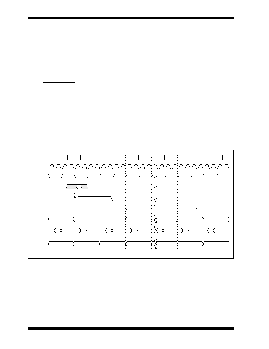
FIGURE 5-5:
INT PIN / T0CKI PIN INTERRUPT TIMING
Q2
Q1
Q3 Q4
Q2
Q1
Q3 Q4
Q2
Q1
Q3 Q4
Q2
Q1
Q3 Q4
Q2
Q1
Q3 Q4
Q2
Q1
Q3 Q4
Q2
Q1
Q3 Q4
OSC1
OSC2
RA0/INT or
RA1/T0CKI
INTF or
T0CKIF
GLINTD
PC
Instruction
executed
System Bus
Instruction
Fetched
PC
PC + 1
Addr (Vector)
PC
Inst (PC)
Inst (PC+1)
Inst (PC)
Dummy
YY
YY + 1
RETFIE
Inst (PC+1)
Inst (Vector)
Addr
Inst (YY + 1)
Dummy
PC + 1
相关PDF资料 |
PDF描述 |
|---|---|
| PALCE16V8Z-25JC | EE CMOS Zero-Power 20-Pin Universal Programmable Array Logic |
| PALCE16V8Z-25JI | EE CMOS Zero-Power 20-Pin Universal Programmable Array Logic |
| PALCE16V8Z-25PC | EE CMOS Zero-Power 20-Pin Universal Programmable Array Logic |
| PALCE16V8Z-25PI | EE CMOS Zero-Power 20-Pin Universal Programmable Array Logic |
| PALCE16V8Z-25SC | EE CMOS Zero-Power 20-Pin Universal Programmable Array Logic |
相关代理商/技术参数 |
参数描述 |
|---|---|
| PIC17LC42A-08/L | 功能描述:8位微控制器 -MCU 4KB 232 RAM 33 I/O RoHS:否 制造商:Silicon Labs 核心:8051 处理器系列:C8051F39x 数据总线宽度:8 bit 最大时钟频率:50 MHz 程序存储器大小:16 KB 数据 RAM 大小:1 KB 片上 ADC:Yes 工作电源电压:1.8 V to 3.6 V 工作温度范围:- 40 C to + 105 C 封装 / 箱体:QFN-20 安装风格:SMD/SMT |
| PIC17LC42A-08/P | 功能描述:8位微控制器 -MCU 4KB 232 RAM 33 I/O RoHS:否 制造商:Silicon Labs 核心:8051 处理器系列:C8051F39x 数据总线宽度:8 bit 最大时钟频率:50 MHz 程序存储器大小:16 KB 数据 RAM 大小:1 KB 片上 ADC:Yes 工作电源电压:1.8 V to 3.6 V 工作温度范围:- 40 C to + 105 C 封装 / 箱体:QFN-20 安装风格:SMD/SMT |
| PIC17LC42A-08/PQ | 功能描述:8位微控制器 -MCU 4KB 232 RAM 33 I/O RoHS:否 制造商:Silicon Labs 核心:8051 处理器系列:C8051F39x 数据总线宽度:8 bit 最大时钟频率:50 MHz 程序存储器大小:16 KB 数据 RAM 大小:1 KB 片上 ADC:Yes 工作电源电压:1.8 V to 3.6 V 工作温度范围:- 40 C to + 105 C 封装 / 箱体:QFN-20 安装风格:SMD/SMT |
| PIC17LC42A-08/PT | 功能描述:8位微控制器 -MCU 4KB 232 RAM 33 I/O RoHS:否 制造商:Silicon Labs 核心:8051 处理器系列:C8051F39x 数据总线宽度:8 bit 最大时钟频率:50 MHz 程序存储器大小:16 KB 数据 RAM 大小:1 KB 片上 ADC:Yes 工作电源电压:1.8 V to 3.6 V 工作温度范围:- 40 C to + 105 C 封装 / 箱体:QFN-20 安装风格:SMD/SMT |
| PIC17LC42A-08I/L | 功能描述:8位微控制器 -MCU 4KB 232 RAM 33 I/O RoHS:否 制造商:Silicon Labs 核心:8051 处理器系列:C8051F39x 数据总线宽度:8 bit 最大时钟频率:50 MHz 程序存储器大小:16 KB 数据 RAM 大小:1 KB 片上 ADC:Yes 工作电源电压:1.8 V to 3.6 V 工作温度范围:- 40 C to + 105 C 封装 / 箱体:QFN-20 安装风格:SMD/SMT |
发布紧急采购,3分钟左右您将得到回复。