- 您现在的位置:买卖IC网 > PDF目录268241 > PIC17CXX (Microchip Technology Inc.) EPROM Memory Programming Specification PDF资料下载
参数资料
| 型号: | PIC17CXX |
| 厂商: | Microchip Technology Inc. |
| 英文描述: | EPROM Memory Programming Specification |
| 中文描述: | EPROM存储器编程规范 |
| 文件页数: | 59/71页 |
| 文件大小: | 1173K |
| 代理商: | PIC17CXX |
第1页第2页第3页第4页第5页第6页第7页第8页第9页第10页第11页第12页第13页第14页第15页第16页第17页第18页第19页第20页第21页第22页第23页第24页第25页第26页第27页第28页第29页第30页第31页第32页第33页第34页第35页第36页第37页第38页第39页第40页第41页第42页第43页第44页第45页第46页第47页第48页第49页第50页第51页第52页第53页第54页第55页第56页第57页第58页当前第59页第60页第61页第62页第63页第64页第65页第66页第67页第68页第69页第70页第71页
PIC17C4X
DS30412C-page 62
1996 Microchip Technology Inc.
9.4.1
PORTE AND DDRE REGISTER
PORTE is a 3-bit bi-directional port. The corresponding
data direction register is DDRE. A '1' in DDRE cong-
ures the corresponding port pin as an input. A '0' in the
DDRE register congures the corresponding port pin
as an output. Reading PORTE reads the status of the
pins, whereas writing to it will write to the port latch.
PORTE is multiplexed with the system bus. When
operating as the system bus, PORTE contains the con-
trol signals for the address/data bus (AD15:AD0).
These control signals are Address Latch Enable (ALE),
Output Enable (OE), and Write (WR). The control sig-
nals OE and WR are active low signals. The timing for
the system bus is shown in the Electrical Characteris-
tics section.
Note:
This port is congured as the system bus
when the device’s conguration bits are
selected to Microprocessor or Extended
Microcontroller modes. In the two other
microcontroller modes, this port is a gen-
eral purpose I/O.
Example 9-4 shows the instruction sequence to initial-
ize PORTE. The Bank Select Register (BSR) must be
selected to Bank 1 for the port to be initialized.
EXAMPLE 9-4:
INITIALIZING PORTE
MOVLB
1
;
Select Bank 1
CLRF
PORTE
;
Initialize PORTE data
;
latches before setting
;
the data direction
;
register
MOVLW
0x03
;
Value used to initialize
;
data direction
MOVWF
DDRE
;
Set RE<1:0> as inputs
;
RE<2> as outputs
;
RE<7:3> are always
;
read as '0'
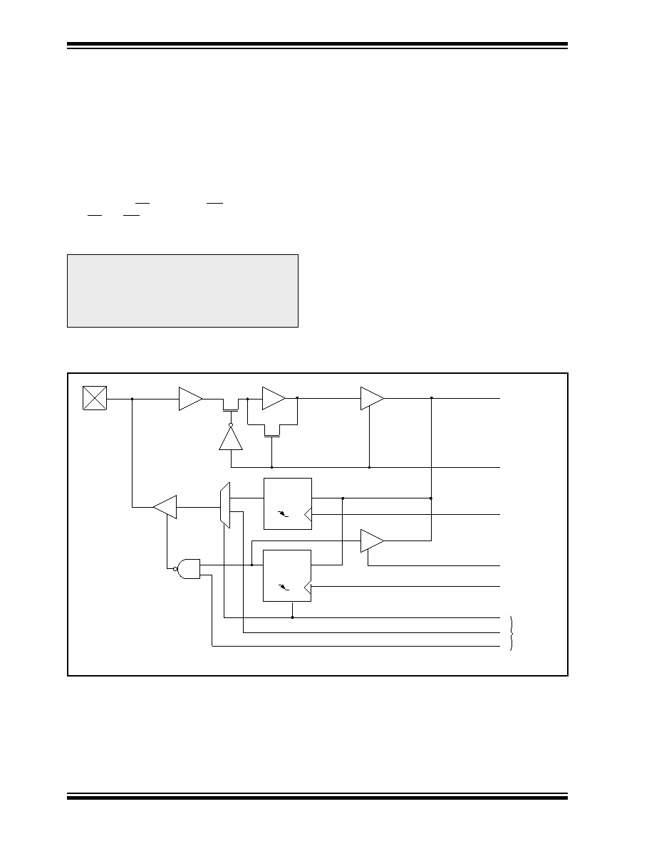
FIGURE 9-8:
PORTE BLOCK DIAGRAM (IN I/O PORT MODE)
Note: I/O pins have protection diodes to VDD and Vss.
Q
D
CK
TTL
0
1
Q
D
CK
R
S
Input
Buffer
Port
Data
Data Bus
RD_PORTE
WR_PORTE
RD_DDRE
WR_DDRE
EX_EN
CNTL
DRV_SYS
SYS BUS
Control
相关PDF资料 |
PDF描述 |
|---|---|
| PALCE16V8Z-25JC | EE CMOS Zero-Power 20-Pin Universal Programmable Array Logic |
| PALCE16V8Z-25JI | EE CMOS Zero-Power 20-Pin Universal Programmable Array Logic |
| PALCE16V8Z-25PC | EE CMOS Zero-Power 20-Pin Universal Programmable Array Logic |
| PALCE16V8Z-25PI | EE CMOS Zero-Power 20-Pin Universal Programmable Array Logic |
| PALCE16V8Z-25SC | EE CMOS Zero-Power 20-Pin Universal Programmable Array Logic |
相关代理商/技术参数 |
参数描述 |
|---|---|
| PIC17LC42A-08/L | 功能描述:8位微控制器 -MCU 4KB 232 RAM 33 I/O RoHS:否 制造商:Silicon Labs 核心:8051 处理器系列:C8051F39x 数据总线宽度:8 bit 最大时钟频率:50 MHz 程序存储器大小:16 KB 数据 RAM 大小:1 KB 片上 ADC:Yes 工作电源电压:1.8 V to 3.6 V 工作温度范围:- 40 C to + 105 C 封装 / 箱体:QFN-20 安装风格:SMD/SMT |
| PIC17LC42A-08/P | 功能描述:8位微控制器 -MCU 4KB 232 RAM 33 I/O RoHS:否 制造商:Silicon Labs 核心:8051 处理器系列:C8051F39x 数据总线宽度:8 bit 最大时钟频率:50 MHz 程序存储器大小:16 KB 数据 RAM 大小:1 KB 片上 ADC:Yes 工作电源电压:1.8 V to 3.6 V 工作温度范围:- 40 C to + 105 C 封装 / 箱体:QFN-20 安装风格:SMD/SMT |
| PIC17LC42A-08/PQ | 功能描述:8位微控制器 -MCU 4KB 232 RAM 33 I/O RoHS:否 制造商:Silicon Labs 核心:8051 处理器系列:C8051F39x 数据总线宽度:8 bit 最大时钟频率:50 MHz 程序存储器大小:16 KB 数据 RAM 大小:1 KB 片上 ADC:Yes 工作电源电压:1.8 V to 3.6 V 工作温度范围:- 40 C to + 105 C 封装 / 箱体:QFN-20 安装风格:SMD/SMT |
| PIC17LC42A-08/PT | 功能描述:8位微控制器 -MCU 4KB 232 RAM 33 I/O RoHS:否 制造商:Silicon Labs 核心:8051 处理器系列:C8051F39x 数据总线宽度:8 bit 最大时钟频率:50 MHz 程序存储器大小:16 KB 数据 RAM 大小:1 KB 片上 ADC:Yes 工作电源电压:1.8 V to 3.6 V 工作温度范围:- 40 C to + 105 C 封装 / 箱体:QFN-20 安装风格:SMD/SMT |
| PIC17LC42A-08I/L | 功能描述:8位微控制器 -MCU 4KB 232 RAM 33 I/O RoHS:否 制造商:Silicon Labs 核心:8051 处理器系列:C8051F39x 数据总线宽度:8 bit 最大时钟频率:50 MHz 程序存储器大小:16 KB 数据 RAM 大小:1 KB 片上 ADC:Yes 工作电源电压:1.8 V to 3.6 V 工作温度范围:- 40 C to + 105 C 封装 / 箱体:QFN-20 安装风格:SMD/SMT |
发布紧急采购,3分钟左右您将得到回复。