- 您现在的位置:买卖IC网 > PDF目录268241 > PIC17CXX (Microchip Technology Inc.) EPROM Memory Programming Specification PDF资料下载
参数资料
| 型号: | PIC17CXX |
| 厂商: | Microchip Technology Inc. |
| 英文描述: | EPROM Memory Programming Specification |
| 中文描述: | EPROM存储器编程规范 |
| 文件页数: | 25/71页 |
| 文件大小: | 1173K |
| 代理商: | PIC17CXX |
第1页第2页第3页第4页第5页第6页第7页第8页第9页第10页第11页第12页第13页第14页第15页第16页第17页第18页第19页第20页第21页第22页第23页第24页当前第25页第26页第27页第28页第29页第30页第31页第32页第33页第34页第35页第36页第37页第38页第39页第40页第41页第42页第43页第44页第45页第46页第47页第48页第49页第50页第51页第52页第53页第54页第55页第56页第57页第58页第59页第60页第61页第62页第63页第64页第65页第66页第67页第68页第69页第70页第71页
1996 Microchip Technology Inc.
DS30412C-page 31
PIC17C4X
6.1.2
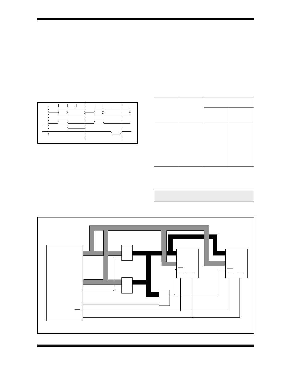
EXTERNAL MEMORY INTERFACE
When either microprocessor or extended microcontrol-
ler mode is selected, PORTC, PORTD and PORTE are
congured as the system bus. PORTC and PORTD are
the multiplexed address/data bus and PORTE is for the
control signals. External components are needed to
demultiplex the address and data. This can be done as
shown in Figure 6-4. The waveforms of address and
data are shown in Figure 6-3. For complete timings,
please refer to the electrical specication section.
FIGURE 6-3:
EXTERNAL PROGRAM
MEMORY ACCESS
WAVEFORMS
The system bus requires that there is no bus conict
(minimal leakage), so the output value (address) will be
capacitively held at the desired value.
As the speed of the processor increases, external
EPROM memory with faster access time must be used.
Table 6-2 lists external memory speed requirements for
a given PIC17C4X device frequency.
Q3
Q1
Q2
Q4
Q3
Q1
Q2
Q4
AD
<15:0>
ALE
OE
WR
'1'
Read cycle
Write cycle
Address out Data in
Address out
Data out
Q1
In extended microcontroller mode, when the device is
executing out of internal memory, the control signals
will continue to be active. That is, they indicate the
action that is occurring in the internal memory. The
external memory access is ignored.
This following selection is for use with Microchip
EPROMs. For interfacing to other manufacturers mem-
ory, please refer to the electrical specications of the
desired PIC17C4X device, as well as the desired mem-
ory device to ensure compatibility.
TABLE 6-2:
EPROM MEMORY ACCESS
TIME ORDERING SUFFIX
PIC17C4X
Oscillator
Frequency
Instruction
Cycle
Time (TCY)
EPROM Sufx
PIC17C42
PIC17C43
PIC17C44
8 MHz
500 ns
-25
16 MHz
250 ns
-12
-15
20 MHz
200 ns
-90
-10
25 MHz
160 ns
N.A.
-70
33 MHz
121 ns
N.A.
(1)
Note 1: The access times for this requires the use of
fast SRAMS.
Note:
The external memory interface is not sup-
ported for the LC devices.
FIGURE 6-4:
TYPICAL EXTERNAL PROGRAM MEMORY CONNECTION DIAGRAM
AD7-AD0
PIC17C4X
AD15-AD8
ALE
I/O(1)
AD15-AD0
373
Memory
(MSB)
Ax-A0
D7-D0
A15-A0
Memory
(LSB)
Ax-A0
D7-D0
373
138(1)
OE
WR
OE
WR
CE
(2)
Note 1:
Use of I/O pins is only required for paged memory.
2:
This signal is unused for ROM and EPROM devices.
相关PDF资料 |
PDF描述 |
|---|---|
| PALCE16V8Z-25JC | EE CMOS Zero-Power 20-Pin Universal Programmable Array Logic |
| PALCE16V8Z-25JI | EE CMOS Zero-Power 20-Pin Universal Programmable Array Logic |
| PALCE16V8Z-25PC | EE CMOS Zero-Power 20-Pin Universal Programmable Array Logic |
| PALCE16V8Z-25PI | EE CMOS Zero-Power 20-Pin Universal Programmable Array Logic |
| PALCE16V8Z-25SC | EE CMOS Zero-Power 20-Pin Universal Programmable Array Logic |
相关代理商/技术参数 |
参数描述 |
|---|---|
| PIC17LC42A-08/L | 功能描述:8位微控制器 -MCU 4KB 232 RAM 33 I/O RoHS:否 制造商:Silicon Labs 核心:8051 处理器系列:C8051F39x 数据总线宽度:8 bit 最大时钟频率:50 MHz 程序存储器大小:16 KB 数据 RAM 大小:1 KB 片上 ADC:Yes 工作电源电压:1.8 V to 3.6 V 工作温度范围:- 40 C to + 105 C 封装 / 箱体:QFN-20 安装风格:SMD/SMT |
| PIC17LC42A-08/P | 功能描述:8位微控制器 -MCU 4KB 232 RAM 33 I/O RoHS:否 制造商:Silicon Labs 核心:8051 处理器系列:C8051F39x 数据总线宽度:8 bit 最大时钟频率:50 MHz 程序存储器大小:16 KB 数据 RAM 大小:1 KB 片上 ADC:Yes 工作电源电压:1.8 V to 3.6 V 工作温度范围:- 40 C to + 105 C 封装 / 箱体:QFN-20 安装风格:SMD/SMT |
| PIC17LC42A-08/PQ | 功能描述:8位微控制器 -MCU 4KB 232 RAM 33 I/O RoHS:否 制造商:Silicon Labs 核心:8051 处理器系列:C8051F39x 数据总线宽度:8 bit 最大时钟频率:50 MHz 程序存储器大小:16 KB 数据 RAM 大小:1 KB 片上 ADC:Yes 工作电源电压:1.8 V to 3.6 V 工作温度范围:- 40 C to + 105 C 封装 / 箱体:QFN-20 安装风格:SMD/SMT |
| PIC17LC42A-08/PT | 功能描述:8位微控制器 -MCU 4KB 232 RAM 33 I/O RoHS:否 制造商:Silicon Labs 核心:8051 处理器系列:C8051F39x 数据总线宽度:8 bit 最大时钟频率:50 MHz 程序存储器大小:16 KB 数据 RAM 大小:1 KB 片上 ADC:Yes 工作电源电压:1.8 V to 3.6 V 工作温度范围:- 40 C to + 105 C 封装 / 箱体:QFN-20 安装风格:SMD/SMT |
| PIC17LC42A-08I/L | 功能描述:8位微控制器 -MCU 4KB 232 RAM 33 I/O RoHS:否 制造商:Silicon Labs 核心:8051 处理器系列:C8051F39x 数据总线宽度:8 bit 最大时钟频率:50 MHz 程序存储器大小:16 KB 数据 RAM 大小:1 KB 片上 ADC:Yes 工作电源电压:1.8 V to 3.6 V 工作温度范围:- 40 C to + 105 C 封装 / 箱体:QFN-20 安装风格:SMD/SMT |
发布紧急采购,3分钟左右您将得到回复。