- 您现在的位置:买卖IC网 > PDF目录268241 > PIC17CXX (Microchip Technology Inc.) EPROM Memory Programming Specification PDF资料下载
参数资料
| 型号: | PIC17CXX |
| 厂商: | Microchip Technology Inc. |
| 英文描述: | EPROM Memory Programming Specification |
| 中文描述: | EPROM存储器编程规范 |
| 文件页数: | 31/71页 |
| 文件大小: | 1173K |
| 代理商: | PIC17CXX |
第1页第2页第3页第4页第5页第6页第7页第8页第9页第10页第11页第12页第13页第14页第15页第16页第17页第18页第19页第20页第21页第22页第23页第24页第25页第26页第27页第28页第29页第30页当前第31页第32页第33页第34页第35页第36页第37页第38页第39页第40页第41页第42页第43页第44页第45页第46页第47页第48页第49页第50页第51页第52页第53页第54页第55页第56页第57页第58页第59页第60页第61页第62页第63页第64页第65页第66页第67页第68页第69页第70页第71页
1996 Microchip Technology Inc.
DS30412C-page 37
PIC17C4X
6.2.2.2
CPU STATUS REGISTER (CPUSTA)
The CPUSTA register contains the status and control
bits for the CPU. This register is used to globally
enable/disable interrupts. If only a specic interrupt is
desired to be enabled/disabled, please refer to the
INTerrupt STAtus (INTSTA) register and the Peripheral
Interrupt Enable (PIE) register. This register also indi-
cates if the stack is available and contains the
Power-down (PD) and Time-out (TO) bits. The TO, PD,
and STKAV bits are not writable. These bits are set and
cleared according to device logic. Therefore, the result
of an instruction with the CPUSTA register as destina-
tion may be different than intended.
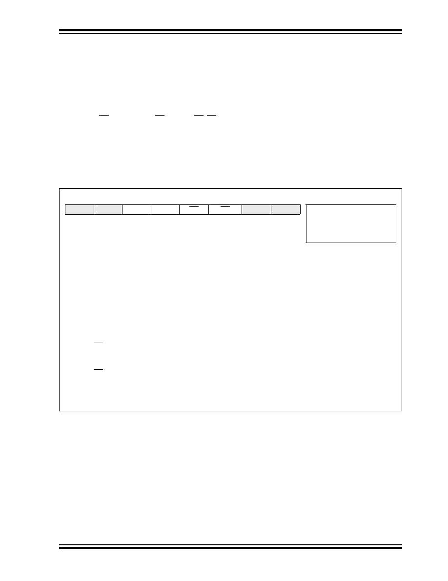
FIGURE 6-8:
CPUSTA REGISTER (ADDRESS: 06h, UNBANKED)
U - 0
R - 1
R/W - 1
R - 1
U - 0
—
STKAV GLINTD
TO
PD
—
R = Readable bit
W = Writable bit
U = Unimplemented bit,
Read as ‘0’
- n = Value at POR reset
bit7
bit0
bit 7-6:
Unimplemented: Read as '0'
bit 5:
STKAV: Stack Available bit
This bit indicates that the 4-bit stack pointer value is Fh, or has rolled over from Fh
→ 0h (stack overow).
1 = Stack is available
0 = Stack is full, or a stack overow may have occurred (Once this bit has been cleared by a
stack overow, only a device reset will set this bit)
bit 4:
GLINTD: Global Interrupt Disable bit
This bit disables all interrupts. When enabling interrupts, only the sources with their enable bits set can
cause an interrupt.
1 = Disable all interrupts
0 = Enables all un-masked interrupts
bit 3:
TO: WDT Time-out Status bit
1 = After power-up or by a CLRWDT instruction
0 = A Watchdog Timer time-out occurred
bit 2:
PD: Power-down Status bit
1 = After power-up or by the CLRWDT instruction
0 = By execution of the SLEEP instruction
bit 1-0:
Unimplemented: Read as '0'
相关PDF资料 |
PDF描述 |
|---|---|
| PALCE16V8Z-25JC | EE CMOS Zero-Power 20-Pin Universal Programmable Array Logic |
| PALCE16V8Z-25JI | EE CMOS Zero-Power 20-Pin Universal Programmable Array Logic |
| PALCE16V8Z-25PC | EE CMOS Zero-Power 20-Pin Universal Programmable Array Logic |
| PALCE16V8Z-25PI | EE CMOS Zero-Power 20-Pin Universal Programmable Array Logic |
| PALCE16V8Z-25SC | EE CMOS Zero-Power 20-Pin Universal Programmable Array Logic |
相关代理商/技术参数 |
参数描述 |
|---|---|
| PIC17LC42A-08/L | 功能描述:8位微控制器 -MCU 4KB 232 RAM 33 I/O RoHS:否 制造商:Silicon Labs 核心:8051 处理器系列:C8051F39x 数据总线宽度:8 bit 最大时钟频率:50 MHz 程序存储器大小:16 KB 数据 RAM 大小:1 KB 片上 ADC:Yes 工作电源电压:1.8 V to 3.6 V 工作温度范围:- 40 C to + 105 C 封装 / 箱体:QFN-20 安装风格:SMD/SMT |
| PIC17LC42A-08/P | 功能描述:8位微控制器 -MCU 4KB 232 RAM 33 I/O RoHS:否 制造商:Silicon Labs 核心:8051 处理器系列:C8051F39x 数据总线宽度:8 bit 最大时钟频率:50 MHz 程序存储器大小:16 KB 数据 RAM 大小:1 KB 片上 ADC:Yes 工作电源电压:1.8 V to 3.6 V 工作温度范围:- 40 C to + 105 C 封装 / 箱体:QFN-20 安装风格:SMD/SMT |
| PIC17LC42A-08/PQ | 功能描述:8位微控制器 -MCU 4KB 232 RAM 33 I/O RoHS:否 制造商:Silicon Labs 核心:8051 处理器系列:C8051F39x 数据总线宽度:8 bit 最大时钟频率:50 MHz 程序存储器大小:16 KB 数据 RAM 大小:1 KB 片上 ADC:Yes 工作电源电压:1.8 V to 3.6 V 工作温度范围:- 40 C to + 105 C 封装 / 箱体:QFN-20 安装风格:SMD/SMT |
| PIC17LC42A-08/PT | 功能描述:8位微控制器 -MCU 4KB 232 RAM 33 I/O RoHS:否 制造商:Silicon Labs 核心:8051 处理器系列:C8051F39x 数据总线宽度:8 bit 最大时钟频率:50 MHz 程序存储器大小:16 KB 数据 RAM 大小:1 KB 片上 ADC:Yes 工作电源电压:1.8 V to 3.6 V 工作温度范围:- 40 C to + 105 C 封装 / 箱体:QFN-20 安装风格:SMD/SMT |
| PIC17LC42A-08I/L | 功能描述:8位微控制器 -MCU 4KB 232 RAM 33 I/O RoHS:否 制造商:Silicon Labs 核心:8051 处理器系列:C8051F39x 数据总线宽度:8 bit 最大时钟频率:50 MHz 程序存储器大小:16 KB 数据 RAM 大小:1 KB 片上 ADC:Yes 工作电源电压:1.8 V to 3.6 V 工作温度范围:- 40 C to + 105 C 封装 / 箱体:QFN-20 安装风格:SMD/SMT |
发布紧急采购,3分钟左右您将得到回复。