- 您现在的位置:买卖IC网 > PDF目录268241 > PIC17CXX (Microchip Technology Inc.) EPROM Memory Programming Specification PDF资料下载
参数资料
| 型号: | PIC17CXX |
| 厂商: | Microchip Technology Inc. |
| 英文描述: | EPROM Memory Programming Specification |
| 中文描述: | EPROM存储器编程规范 |
| 文件页数: | 6/71页 |
| 文件大小: | 1173K |
| 代理商: | PIC17CXX |
第1页第2页第3页第4页第5页当前第6页第7页第8页第9页第10页第11页第12页第13页第14页第15页第16页第17页第18页第19页第20页第21页第22页第23页第24页第25页第26页第27页第28页第29页第30页第31页第32页第33页第34页第35页第36页第37页第38页第39页第40页第41页第42页第43页第44页第45页第46页第47页第48页第49页第50页第51页第52页第53页第54页第55页第56页第57页第58页第59页第60页第61页第62页第63页第64页第65页第66页第67页第68页第69页第70页第71页
PIC17C4X
DS30412C-page 14
1996 Microchip Technology Inc.
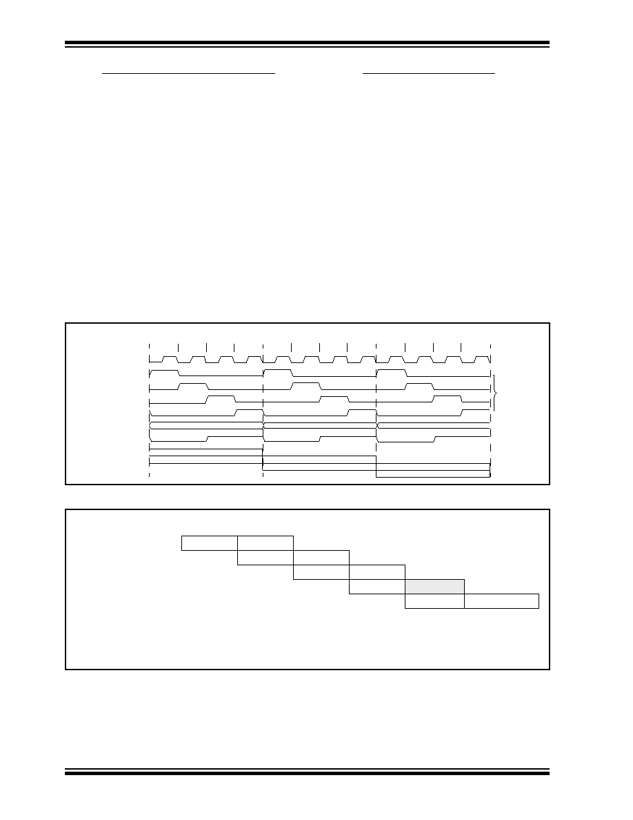
3.1
Clocking Scheme/Instruction Cycle
The clock input (from OSC1) is internally divided by
four to generate four non-overlapping quadrature
clocks, namely Q1, Q2, Q3, and Q4. Internally, the pro-
gram counter (PC) is incremented every Q1, and the
instruction is fetched from the program memory and
latched into the instruction register in Q4. The instruc-
tion is decoded and executed during the following Q1
through Q4. The clocks and instruction execution ow
are shown in Figure 3-3.
3.2
Instruction Flow/Pipelining
An “Instruction Cycle” consists of four Q cycles (Q1,
Q2, Q3, and Q4). The instruction fetch and execute are
pipelined such that fetch takes one instruction cycle
while decode and execute takes another instruction
cycle. However, due to the pipelining, each instruction
effectively executes in one cycle. If an instruction
causes the program counter to change (e.g.GOTO) then
two cycles are required to complete the instruction
A fetch cycle begins with the program counter incre-
menting in Q1.
In the execution cycle, the fetched instruction is latched
into the “Instruction Register (IR)” in cycle Q1. This
instruction is then decoded and executed during the
Q2, Q3, and Q4 cycles. Data memory is read during Q2
(operand read) and written during Q4 (destination
write).
FIGURE 3-3:
CLOCK/INSTRUCTION CYCLE
EXAMPLE 3-2:
INSTRUCTION PIPELINE FLOW
Q1
Q2
Q3
Q4
Q1
Q2
Q3
Q4
Q1
Q2
Q3
Q4
OSC1
Q1
Q2
Q3
Q4
PC
OSC2/CLKOUT
(RC mode)
PC
PC+1
PC+2
Fetch INST (PC)
Execute INST (PC-1)
Fetch INST (PC+1)
Execute INST (PC)
Fetch INST (PC+2)
Execute INST (PC+1)
Internal
phase
clock
All instructions are single cycle, except for any program branches. These take two cycles since the fetch
instruction is “ushed” from the pipeline while the new instruction is being fetched and then executed.
Tcy0
Tcy1
Tcy2
Tcy3
Tcy4
Tcy5
1. MOVLW 55h
Fetch 1
Execute 1
2. MOVWF PORTB
Fetch 2
Execute 2
3. CALL SUB_1
Fetch 3
Execute 3
4. BSF
PORTA, BIT3 (Forced NOP)
Fetch 4
Flush
5. Instruction @ address SUB_1
Fetch SUB_1 Execute SUB_1
相关PDF资料 |
PDF描述 |
|---|---|
| PALCE16V8Z-25JC | EE CMOS Zero-Power 20-Pin Universal Programmable Array Logic |
| PALCE16V8Z-25JI | EE CMOS Zero-Power 20-Pin Universal Programmable Array Logic |
| PALCE16V8Z-25PC | EE CMOS Zero-Power 20-Pin Universal Programmable Array Logic |
| PALCE16V8Z-25PI | EE CMOS Zero-Power 20-Pin Universal Programmable Array Logic |
| PALCE16V8Z-25SC | EE CMOS Zero-Power 20-Pin Universal Programmable Array Logic |
相关代理商/技术参数 |
参数描述 |
|---|---|
| PIC17LC42A-08/L | 功能描述:8位微控制器 -MCU 4KB 232 RAM 33 I/O RoHS:否 制造商:Silicon Labs 核心:8051 处理器系列:C8051F39x 数据总线宽度:8 bit 最大时钟频率:50 MHz 程序存储器大小:16 KB 数据 RAM 大小:1 KB 片上 ADC:Yes 工作电源电压:1.8 V to 3.6 V 工作温度范围:- 40 C to + 105 C 封装 / 箱体:QFN-20 安装风格:SMD/SMT |
| PIC17LC42A-08/P | 功能描述:8位微控制器 -MCU 4KB 232 RAM 33 I/O RoHS:否 制造商:Silicon Labs 核心:8051 处理器系列:C8051F39x 数据总线宽度:8 bit 最大时钟频率:50 MHz 程序存储器大小:16 KB 数据 RAM 大小:1 KB 片上 ADC:Yes 工作电源电压:1.8 V to 3.6 V 工作温度范围:- 40 C to + 105 C 封装 / 箱体:QFN-20 安装风格:SMD/SMT |
| PIC17LC42A-08/PQ | 功能描述:8位微控制器 -MCU 4KB 232 RAM 33 I/O RoHS:否 制造商:Silicon Labs 核心:8051 处理器系列:C8051F39x 数据总线宽度:8 bit 最大时钟频率:50 MHz 程序存储器大小:16 KB 数据 RAM 大小:1 KB 片上 ADC:Yes 工作电源电压:1.8 V to 3.6 V 工作温度范围:- 40 C to + 105 C 封装 / 箱体:QFN-20 安装风格:SMD/SMT |
| PIC17LC42A-08/PT | 功能描述:8位微控制器 -MCU 4KB 232 RAM 33 I/O RoHS:否 制造商:Silicon Labs 核心:8051 处理器系列:C8051F39x 数据总线宽度:8 bit 最大时钟频率:50 MHz 程序存储器大小:16 KB 数据 RAM 大小:1 KB 片上 ADC:Yes 工作电源电压:1.8 V to 3.6 V 工作温度范围:- 40 C to + 105 C 封装 / 箱体:QFN-20 安装风格:SMD/SMT |
| PIC17LC42A-08I/L | 功能描述:8位微控制器 -MCU 4KB 232 RAM 33 I/O RoHS:否 制造商:Silicon Labs 核心:8051 处理器系列:C8051F39x 数据总线宽度:8 bit 最大时钟频率:50 MHz 程序存储器大小:16 KB 数据 RAM 大小:1 KB 片上 ADC:Yes 工作电源电压:1.8 V to 3.6 V 工作温度范围:- 40 C to + 105 C 封装 / 箱体:QFN-20 安装风格:SMD/SMT |
发布紧急采购,3分钟左右您将得到回复。