- 您现在的位置:买卖IC网 > PDF目录378056 > PM73488-PI (PMC-SIERRA INC) 5 Gbit/s ATM Switch Fabric Element PDF资料下载
参数资料
| 型号: | PM73488-PI |
| 厂商: | PMC-SIERRA INC |
| 元件分类: | 数字传输电路 |
| 英文描述: | 5 Gbit/s ATM Switch Fabric Element |
| 中文描述: | ATM SWITCHING CIRCUIT, PBGA596 |
| 封装: | EPBGA-596 |
| 文件页数: | 70/135页 |
| 文件大小: | 1735K |
| 代理商: | PM73488-PI |
第1页第2页第3页第4页第5页第6页第7页第8页第9页第10页第11页第12页第13页第14页第15页第16页第17页第18页第19页第20页第21页第22页第23页第24页第25页第26页第27页第28页第29页第30页第31页第32页第33页第34页第35页第36页第37页第38页第39页第40页第41页第42页第43页第44页第45页第46页第47页第48页第49页第50页第51页第52页第53页第54页第55页第56页第57页第58页第59页第60页第61页第62页第63页第64页第65页第66页第67页第68页第69页当前第70页第71页第72页第73页第74页第75页第76页第77页第78页第79页第80页第81页第82页第83页第84页第85页第86页第87页第88页第89页第90页第91页第92页第93页第94页第95页第96页第97页第98页第99页第100页第101页第102页第103页第104页第105页第106页第107页第108页第109页第110页第111页第112页第113页第114页第115页第116页第117页第118页第119页第120页第121页第122页第123页第124页第125页第126页第127页第128页第129页第130页第131页第132页第133页第134页第135页
PMC-Sierra, Inc.
PM73488 QSE
L
PMC-980616
Issue 3
5 Gbit/s ATMSwitch Fabric Element
Released
Datasheet
72
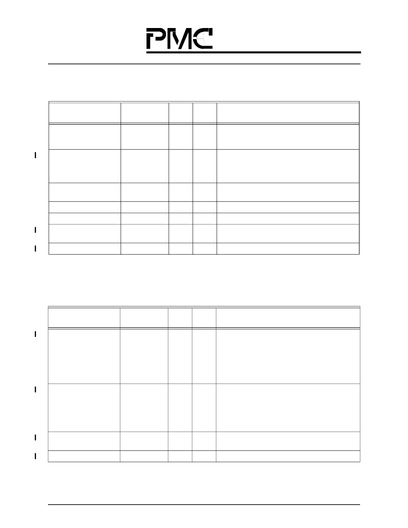
6.4.1
Processor Interface Signals
Table 16. Processor Interface Signals (21 Signal Pins)
Signal Name
Ball
#
# of
Pins
Type
Description
ADD(7:0)
AJ7, AH9, AG10,
AF10, AK4, AH8,
AG9, AK3
8
In
Address Bits 7to 0
are part of the 8-bit processor address
bus.
DATA(7:0)
AJ9, AH10,
AG11, AE13,
AE12, AJ8, AF11,
AK6
8
Bi 3
Data Bits 7 to 0 are
part of the 8-bit processor data bus.
/CS
AK7
1
In
Chip Select
is an active low signal that selects the device
for processor access.
/RD
AK8
1
In
Read
is an active low signal that selects a read cycle.
/WR
AH12
1
In
Write
is an active low signal that selects a write cycle.
/ACK
AJ11
1
Out 5
Acknowledge
is an active low signal that indicates the
processor cycle is finished.
/INTR
AG13
1
Out 5
Interrupt
indicates an interrupt is present.
6.4.2
Multicast RAM Interface Signals
Table 17. Multicast RAM Interface Signals (39 Signal Pins)
Signal Name
Ball
#
# of
Pins
Type
Description
RAM_ADD(18:0)
AF12, AH1, F18,
C27, E23, E24,
D24, F24, D26,
D25, E25, A29,
B30, F26, F27,
E27, G25, G27,
G26
19
Out 5
RAM Address Bits 18 to 0
are part of the 19-bit SRAM
address bus.
RAM_DATA(15:0)
C22, E20, A27,
B24, D22, D21,
E21, E22, C23,
B27, A28, C25,
B26, F21, B28,
F22
16
Bi 3
RAM Data Bits 15 to 0 are
part of the 16-bit SRAM data
bus.
RAM_PARITY
F19
1
Bi 3
Parity for the RAM Data bits. Generated and checked by
the QSE.
B23
1
Out 8
RAM Clock.
相关PDF资料 |
PDF描述 |
|---|---|
| PM73488 | 5 Gbit/s ATM Switch Fabric Element |
| PM7349 | Ultraframer DS3/E3/DS2/E2/DS1/E1/DS0 |
| PM7350 | Dual Serial Link, PHY Multiplexer |
| PM7350-PI | DUAL SERIAL LINK PHY MULTIPLEXER |
| PM7351 | OCTAL SERIAL LINK MULTIPLEXER |
相关代理商/技术参数 |
参数描述 |
|---|---|
| PM7349 | 制造商:PMC 制造商全称:PMC 功能描述:Quad J2, E3 and DS-3 Framer |
| PM7349-BI | 制造商:未知厂家 制造商全称:未知厂家 功能描述:Telecommunication IC |
| PM7350 | 制造商:PMC 制造商全称:PMC 功能描述:DUAL SERIAL LINK PHY MULTIPLEXER |
发布紧急采购,3分钟左右您将得到回复。