- 您现在的位置:买卖IC网 > PDF目录69321 > RTPXA270C5C520 (INTEL CORP) 32-BIT, 520 MHz, RISC PROCESSOR, PBGA356 PDF资料下载
参数资料
| 型号: | RTPXA270C5C520 |
| 厂商: | INTEL CORP |
| 元件分类: | 微控制器/微处理器 |
| 英文描述: | 32-BIT, 520 MHz, RISC PROCESSOR, PBGA356 |
| 封装: | 13 X 13 MM, 1.0MM PITCH, LEAD FREE, VFBGA-356 |
| 文件页数: | 2/44页 |
| 文件大小: | 1302K |
| 代理商: | RTPXA270C5C520 |
第1页当前第2页第3页第4页第5页第6页第7页第8页第9页第10页第11页第12页第13页第14页第15页第16页第17页第18页第19页第20页第21页第22页第23页第24页第25页第26页第27页第28页第29页第30页第31页第32页第33页第34页第35页第36页第37页第38页第39页第40页第41页第42页第43页第44页
Package Information
10
Intel PXA255 Processor Electrical, Mechanical, and Thermal Specification
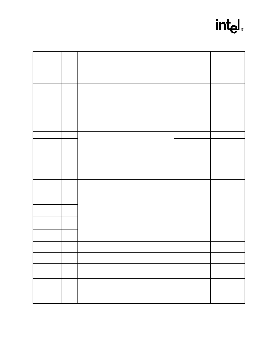
SDCKE[1]
OC
SDRAM and/or Synchronous Static Memory clock
enable. (output) Connect to the clock enable pins of
SDRAM. It is deasserted during sleep. SDCKE[1] is
always de-asserted upon reset. The memory controller
provides control register bits for de-assertion.
Driven low
SDCLK[0]
OC
Synchronous Static Memory clock. (output) Connect to
the clock (CLK) pins of SMROM. It is driven by either the
internal memory controller clock, or the internal memory
controller clock divided by 2. At reset, all clock pins are
free running at the divide-by-2 clock speed and may be
turned off via free-running control register bits in the
memory controller. The memory controller also provides
control register bits for clock division and deassertion of
each SDCLK pin. SDCLK[0] control register assertion bit
defaults to on if the boot-time static memory bank 0 is
configured for SMROM.
SDCLK[1]
OCZ
SDRAM Clocks (output) Connect SDCLK[1] and
SDCLK[2] to the clock pins of SDRAM in bank pairs 0/1
and 2/3, respectively. They are driven by either the
internal memory controller clock, or the internal memory
controller clock divided by 2. At reset, all clock pins are
free running at the divide-by-2 clock speed and may be
turned off via free-running control register bits in the
memory controller. The memory controller also provides
control register bits for clock division and de-assertion of
each SDCLK pin. SDCLK[2:1] control register assertion
bits are always de-asserted upon reset.
Driven Low
SDCLK[2]
OC
Driven Low
nCS[5]/
GPIO[33]
ICOCZ
Static chip selects. (output) Chip selects to static
memory devices such as ROM and Flash. Individually
programmable in the memory configuration registers.
nCS[5:0] can be used with variable latency I/O devices.
Pulled High -
Note[1]
Note [4]
nCS[4]/
GPIO[80]
ICOCZ
nCS[3]/
GPIO[79]
ICOCZ
nCS[2]/
GPIO[78]
ICOCZ
nCS[1]/
GPIO[15]
ICOCZ
nCS[0]
ICOCZ
Static chip select 0. (output) Chip select for the boot
memory. nCS[0] is a dedicated pin.
Driven High
Note [4]
RD/nWR
OCZ
Read/Write for static interface. (output) Signals that the
current transaction is a read or write.
Driven Low
Holds last state
RDY/
GPIO[18]
ICOCZ
Variable latency I/O ready pin. (input) Notifies the
memory controller when an external bus device is ready
to transfer data.
Pulled High -
Note[1]
Note [3]
L_DD[8]/
GPIO[66]
ICOCZ
LCD display data. (output) Transfers pixel information
from the LCD controller to the external LCD panel.
Memory controller alternate bus master request.
(input) Allows an external device to request the system
bus from the memory controller.
Pulled High -
Note[1]
Note [3]
Table 3. Pin and Signal Descriptions for the PXA255 Processor (Sheet 2 of 9)
Pin Name
Type
Signal Descriptions
Reset State
Sleep State
相关PDF资料 |
PDF描述 |
|---|---|
| RCPXA272FC0520 | 520 MHz, MICROPROCESSOR, PBGA336 |
| RCPXA273FC0416 | 416 MHz, MICROPROCESSOR, PBGA336 |
| RCPXA273FC0520 | 520 MHz, MICROPROCESSOR, PBGA336 |
| RCPXA272FC0312 | 312 MHz, MICROPROCESSOR, PBGA336 |
| RCPXA271FC0312 | 312 MHz, MICROPROCESSOR, PBGA336 |
相关代理商/技术参数 |
参数描述 |
|---|---|
| RTPXA270C5C624 | 功能描述:IC MPU 32BIT 624MHZ 356-PBGA RoHS:是 类别:集成电路 (IC) >> 嵌入式 - 微处理器 系列:- 标准包装:1 系列:MPC85xx 处理器类型:32-位 MPC85xx PowerQUICC III 特点:- 速度:1.2GHz 电压:1.1V 安装类型:表面贴装 封装/外壳:783-BBGA,FCBGA 供应商设备封装:783-FCPBGA(29x29) 包装:托盘 |
| RTPXA320B1C624-180 | 制造商:Marvell 功能描述:MONAHANS P 624MHZ - Trays |
| RTPXA320B1C624-203 | 制造商:Marvell 功能描述:MONAHANS P 624MHZ - Trays |
| RTPXA320B1C624-208 | 制造商:Marvell 功能描述:MONAHANS P 624MHZ - Trays |
| RTPXA320B1C624-209 | 制造商:Marvell 功能描述:MONAHANS P 624MHZ - Trays |
发布紧急采购,3分钟左右您将得到回复。