- 您现在的位置:买卖IC网 > PDF目录192295 > S29AL032D70BAE002 (Spansion Inc.) 32 Megabit CMOS 3.0 Volt-only Flash Memory PDF资料下载
参数资料
| 型号: | S29AL032D70BAE002 |
| 厂商: | Spansion Inc. |
| 英文描述: | 32 Megabit CMOS 3.0 Volt-only Flash Memory |
| 中文描述: | 32兆位的CMOS 3.0伏只闪存 |
| 文件页数: | 22/69页 |
| 文件大小: | 1970K |
| 代理商: | S29AL032D70BAE002 |
第1页第2页第3页第4页第5页第6页第7页第8页第9页第10页第11页第12页第13页第14页第15页第16页第17页第18页第19页第20页第21页当前第22页第23页第24页第25页第26页第27页第28页第29页第30页第31页第32页第33页第34页第35页第36页第37页第38页第39页第40页第41页第42页第43页第44页第45页第46页第47页第48页第49页第50页第51页第52页第53页第54页第55页第56页第57页第58页第59页第60页第61页第62页第63页第64页第65页第66页第67页第68页第69页
June 13, 2005 S29AL032D_00_A3
S29AL032D
27
Ad vance
Info rmat i o n
without raising any device pin to a high voltage. Note that this method is only applicable to
the Secured Silicon Sector.
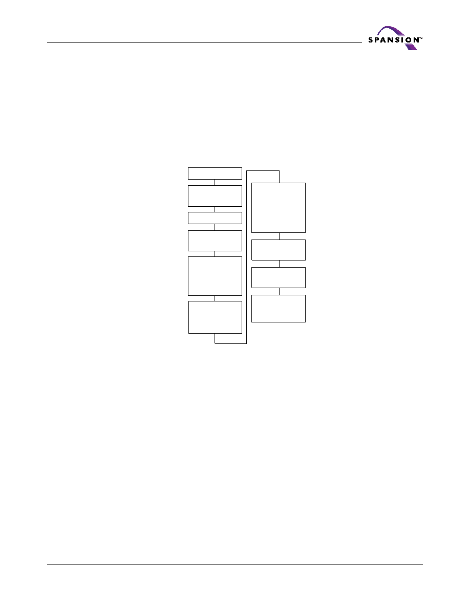
To verify the protect/unprotect status of the Secured Silicon Sector, follow the algorithm
shown in Figure 3, on page 27.
Once the Secured Silicon Sector is locked and verified, the system must write the Exit Secured
Silicon Sector Region command sequence to return to reading and writing the remainder of the
array.
The Secured Silicon Sector protection must be used with caution since, once protected, there is
no procedure available for unprotecting the Secured Silicon Sector area and none of the bits in
the Secured Silicon Sector memory space can be modified in any way.
Figure 3. Secured Silicon Sector Protect Verify
Hardware Data Protection
The command sequence requirement of unlock cycles for programming or erasing provides data
protection against inadvertent writes (refer to Table 17 on page 38 for command definitions). In
addition, the following hardware data protection measures prevent accidental erasure or pro-
gramming, which might otherwise be caused by spurious system level signals during VCC
power-up and power-down transitions, or from system noise.
Low VCC Write Inhibit
When VCC is less than VLKO, the device does not accept any write cycles. This protects data during
VCC power-up and power-down. The command register and all internal program/erase circuits are
disabled, and the device resets. Subsequent writes are ignored until VCC is greater than VLKO. The
system must provide the proper signals to the control pins to prevent unintentional writes when
VCC is greater than VLKO.
Write Pulse “Glitch” Protection
Noise pulses of less than 5 ns (typical) on OE#, CE# or WE# do not initiate a write cycle.
Logical Inhibit
Write cycles are inhibited by holding any one of OE# = VIL, CE# = VIH or WE# = VIH. To initiate
a write cycle, CE# and WE# must be a logical zero while OE# is a logical one.
Write 60h to
any address
Write 40h to SecSi
Sector address
with A6 = 0,
A1 = 1, A0 = 0
START
RESET# =
VIH or VID
Wait 1
μs
Read from SecSi
Sector address
with A6 = 0,
A1 = 1, A0 = 0
If data = 00h,
SecSi Sector is
unprotected.
If data = 01h,
SecSi Sector is
protected.
Remove VIH or VID
from RESET#
Write reset
command
SecSi Sector
Protect Verify
complete
相关PDF资料 |
PDF描述 |
|---|---|
| S29AL032D90TFI042 | 32 Megabit CMOS 3.0 Volt-only Flash Memory |
| S29AL032D90TFI043 | 32 Megabit CMOS 3.0 Volt-only Flash Memory |
| S29CD016G0JDEI004 | 512K X 32 FLASH 2.7V PROM, 67 ns, UUC76 |
| S29CD016G0JDEI007 | 512K X 32 FLASH 2.7V PROM, 67 ns, UUC76 |
| S29CD032J1JFAI122 | 1M X 32 FLASH 2.7V PROM, 54 ns, PBGA80 |
相关代理商/技术参数 |
参数描述 |
|---|---|
| S29AL032D70BAI000 | 制造商:Spansion 功能描述:NOR Flash Parallel 3.3V 32Mbit 4M x 8bit 70ns 48-Pin FBGA Tray |
| S29AL032D70BAI030 | 制造商:Spansion 功能描述:NOR Flash Parallel 3V/3.3V 32Mbit 4M/2M x 8bit/16bit 70ns 48-Pin FBGA Tray |
| S29AL032D70BAI032 | 制造商:Spansion 功能描述:NOR Flash Parallel 3V/3.3V 32Mbit 4M/2M x 8bit/16bit 70ns 48-Pin FBGA T/R |
| S29AL032D70BFI000 | 功能描述:闪存 32MB 闪存 3V 70ns Parallel NOR 闪存 RoHS:否 制造商:ON Semiconductor 数据总线宽度:1 bit 存储类型:Flash 存储容量:2 MB 结构:256 K x 8 定时类型: 接口类型:SPI 访问时间: 电源电压-最大:3.6 V 电源电压-最小:2.3 V 最大工作电流:15 mA 工作温度:- 40 C to + 85 C 安装风格:SMD/SMT 封装 / 箱体: 封装:Reel |
| S29AL032D70BFI030 | 功能描述:闪存 32MB 闪存 3V 70ns Parallel NOR 闪存 RoHS:否 制造商:ON Semiconductor 数据总线宽度:1 bit 存储类型:Flash 存储容量:2 MB 结构:256 K x 8 定时类型: 接口类型:SPI 访问时间: 电源电压-最大:3.6 V 电源电压-最小:2.3 V 最大工作电流:15 mA 工作温度:- 40 C to + 85 C 安装风格:SMD/SMT 封装 / 箱体: 封装:Reel |
发布紧急采购,3分钟左右您将得到回复。