- 您现在的位置:买卖IC网 > PDF目录225140 > S29CD016G0MFAN002 (SPANSION LLC) 16 Megabit (512 K x 32-Bit) CMOS 2.5 Volt-only Burst Mode, Dual Boot, Simultaneous Read/Write Flash Memory PDF资料下载
参数资料
| 型号: | S29CD016G0MFAN002 |
| 厂商: | SPANSION LLC |
| 元件分类: | PROM |
| 英文描述: | 16 Megabit (512 K x 32-Bit) CMOS 2.5 Volt-only Burst Mode, Dual Boot, Simultaneous Read/Write Flash Memory |
| 中文描述: | 512K X 32 FLASH 2.7V PROM, 64 ns, PBGA80 |
| 封装: | 13 X 11 MM, 1 MM PITCH, FORTIFIED, BGA-80 |
| 文件页数: | 40/81页 |
| 文件大小: | 1276K |
| 代理商: | S29CD016G0MFAN002 |
第1页第2页第3页第4页第5页第6页第7页第8页第9页第10页第11页第12页第13页第14页第15页第16页第17页第18页第19页第20页第21页第22页第23页第24页第25页第26页第27页第28页第29页第30页第31页第32页第33页第34页第35页第36页第37页第38页第39页当前第40页第41页第42页第43页第44页第45页第46页第47页第48页第49页第50页第51页第52页第53页第54页第55页第56页第57页第58页第59页第60页第61页第62页第63页第64页第65页第66页第67页第68页第69页第70页第71页第72页第73页第74页第75页第76页第77页第78页第79页第80页第81页
March 3, 2009 S29CD-G_00_B1
S29CD-G Flash Family
43
Da ta
Shee t
(Prelim i nar y )
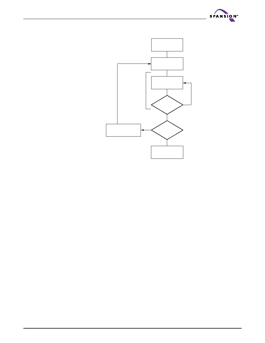
Figure 15.1 Program Operation
Note
See Table 15.2 on page 52 and Table 15.3 on page 53 for program command sequence.
15.7.1
Unlock Bypass Entry Command
The Unlock Bypass command, once issued, is used to bypass the unlock sequence for program, chip erase,
and CFI commands. This feature permits slow PROM programmers to significantly improve programming/
erase throughput since the command sequence often requires microseconds to execute a single write
operation. Therefore, once the Unlock Bypass command is issued, only the two-cycle program and erase
bypass commands are required. The Unlock Bypass Command is ignored if the Secured Silicon sector is
enabled. To return back to normal operation, the Unlock Bypass Reset Command must be issued.
The following four sections describe the commands that may be executed within the unlock bypass mode.
15.7.2
Unlock Bypass Program Command
The Unlock Bypass Program command is a two-cycle command that consists of the actual program
command (A0h) and the program address/data combination. This command does not require the two-cycle
unlock sequence since the Unlock Bypass command was previously issued. As with the standard program
command, multiple Unlock Bypass Program commands can be issued once the Unlock Bypass command is
issued.
To return back to standard read operations, the Unlock Bypass Reset command must be issued.
The Unlock Bypass Program Command is ignored if the Secured Silicon sector is enabled.
15.7.3
Unlock Bypass Chip Erase Command
The Unlock Bypass Chip Erase command is a 2-cycle command that consists of the erase setup command
(80h) and the actual chip erase command (10h). This command does not require the two-cycle unlock
sequence since the Unlock Bypass command was previously issued. Unlike the standard erase command,
there is no Unlock Bypass Erase Suspend or Erase Resume commands.
To return back to standard read operations, the Unlock Bypass Reset command must be issued.
The Unlock Bypass Program Command is ignored if the Secured Silicon sector is enabled.
START
Write Program
Command Sequence
Data Poll
from System
Verify Data?
No
Yes
Last Address?
No
Yes
Programming
Completed
Increment Address
Embedded
Program
algorithm
in progress
相关PDF资料 |
PDF描述 |
|---|---|
| S29CD016G0MFAN003 | 16 Megabit (512 K x 32-Bit) CMOS 2.5 Volt-only Burst Mode, Dual Boot, Simultaneous Read/Write Flash Memory |
| S29CD016G0MFAN010 | 16 Megabit (512 K x 32-Bit) CMOS 2.5 Volt-only Burst Mode, Dual Boot, Simultaneous Read/Write Flash Memory |
| S29CD032G0JFFN002 | 1M X 32 FLASH 2.7V PROM, 67 ns, PBGA80 |
| S29CD032G0RFFN003 | 1M X 32 FLASH 2.7V PROM, 48 ns, PBGA80 |
| S29CD032G0RQFI012 | 1M X 32 FLASH 2.7V PROM, 48 ns, PQFP80 |
相关代理商/技术参数 |
参数描述 |
|---|---|
| S29CD016G0MFAN003 | 制造商:SPANSION 制造商全称:SPANSION 功能描述:16 Megabit (512 K x 32-Bit) CMOS 2.5 Volt-only Burst Mode, Dual Boot, Simultaneous Read/Write Flash Memory |
| S29CD016G0MFAN010 | 制造商:SPANSION 制造商全称:SPANSION 功能描述:16 Megabit (512 K x 32-Bit) CMOS 2.5 Volt-only Burst Mode, Dual Boot, Simultaneous Read/Write Flash Memory |
| S29CD016G0MFAN011 | 制造商:SPANSION 制造商全称:SPANSION 功能描述:16 Megabit (512 K x 32-Bit) CMOS 2.5 Volt-only Burst Mode, Dual Boot, Simultaneous Read/Write Flash Memory |
| S29CD016G0MFAN012 | 制造商:SPANSION 制造商全称:SPANSION 功能描述:16 Megabit (512 K x 32-Bit) CMOS 2.5 Volt-only Burst Mode, Dual Boot, Simultaneous Read/Write Flash Memory |
| S29CD016G0MFAN013 | 制造商:SPANSION 制造商全称:SPANSION 功能描述:16 Megabit (512 K x 32-Bit) CMOS 2.5 Volt-only Burst Mode, Dual Boot, Simultaneous Read/Write Flash Memory |
发布紧急采购,3分钟左右您将得到回复。