- 您现在的位置:买卖IC网 > PDF目录11825 > SC16C2552BIA44,512 (NXP Semiconductors)IC UART DUAL SOT187-2 PDF资料下载
参数资料
| 型号: | SC16C2552BIA44,512 |
| 厂商: | NXP Semiconductors |
| 文件页数: | 36/37页 |
| 文件大小: | 0K |
| 描述: | IC UART DUAL SOT187-2 |
| 标准包装: | 26 |
| 特点: | 2 通道 |
| 通道数: | 2,DUART |
| FIFO's: | 16 字节 |
| 电源电压: | 2.5V,3.3V,5V |
| 带IrDA 编码器/解码器: | 是 |
| 带故障启动位检测功能: | 是 |
| 带调制解调器控制功能: | 是 |
| 带CMOS: | 是 |
| 安装类型: | 表面贴装 |
| 封装/外壳: | 44-LCC(J 形引线) |
| 供应商设备封装: | 44-PLCC |
| 包装: | 管件 |
| 其它名称: | 935274408512 SC16C2552BIA44 SC16C2552BIA44-ND |
第1页第2页第3页第4页第5页第6页第7页第8页第9页第10页第11页第12页第13页第14页第15页第16页第17页第18页第19页第20页第21页第22页第23页第24页第25页第26页第27页第28页第29页第30页第31页第32页第33页第34页第35页当前第36页第37页
SC16C2552B_3
NXP B.V. 2009. All rights reserved.
Product data sheet
Rev. 03 — 12 February 2009
8 of 38
NXP Semiconductors
SC16C2552B
5 V, 3.3 V and 2.5 V dual UART, 5 Mbit/s (max.), with 16-byte FIFOs
When two interrupt conditions have the same priority, it is important to service these
interrupts correctly. Receive Data Ready and Receive Time-Out have the same interrupt
priority (when enabled by IER[0]). The receiver issues an interrupt after the number of
characters have reached the programmed trigger level. In this case, the SC16C2552B
FIFO may hold more characters than the programmed trigger level. Following the removal
of a data byte, the user should re-check LSR[0] for additional characters. A Receive
Time-Out will not occur if the receive FIFO is empty. The time-out counter is reset at the
center of each stop bit received or each time the receive holding register (RHR) is read.
The actual time-out value is 4 character time.
6.5 Programmable baud rate generator
The SC16C2552B supports high speed modem technologies that have increased input
data rates by employing data compression schemes. For example, a 33.6 kbit/s modem
that employs data compression may require a 115.2 kbit/s input data rate. A 128.0 kbit/s
ISDN modem that supports data compression may need an input data rate of 460.8 kbit/s.
A baud rate generator is provided for each UART channel, allowing independent TX/RX
channel control. The programmable Baud Rate Generator (BRG) is capable of accepting
an input clock up to 80 MHz, as required for supporting a 5 Mbit/s data rate. The
SC16C2552B can be congured for internal or external clock operation. For internal clock
oscillator operation, an industry standard microprocessor crystal is connected externally
between the XTAL1 and XTAL2 pins. Alternatively, an external clock can be connected to
the XTAL1 pin to clock the internal baud rate generator for standard or custom rates (see
Table 5).
The generator divides the input 16
× clock by any divisor from 1 to (216 1). The
SC16C2552B divides the basic external clock by 16. The basic 16
× clock provides table
rates to support standard and custom applications using the same system design. The
rate table is congured via the DLL and DLM internal register functions. Customized baud
rates can be achieved by selecting the proper divisor values for the MSB and LSB
sections of baud rate generator.
Programming the baud rate generator registers DLM (MSB) and DLL (LSB) provides a
user capability for selecting the desired nal baud rate. The example in Table 5 shows the
selectable baud rate table available when using a 1.8432 MHz external clock input.
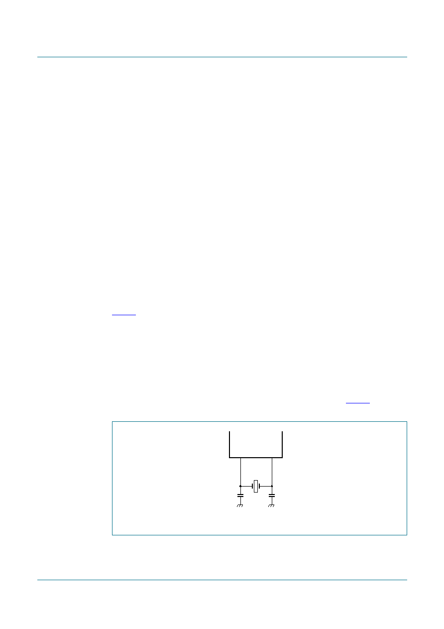
Fig 3.
Crystal oscillator connection
002aab325
C2
33 pF
XTAL1
XTAL2
X1
1.8432 MHz
C1
22 pF
相关PDF资料 |
PDF描述 |
|---|---|
| SC16C652BIBS,157 | IC UART DUAL W/FIFO 32HVQFN |
| VI-23R-IY | CONVERTER MOD DC/DC 7.5V 50W |
| SC16C852VIET,157 | IC UART DUAL W/FIFO 36TFBGA |
| MS3102R32-8S | CONN RCPT 30POS BOX MNT W/SCKT |
| MS3102E32-8S | CONN RCPT 30POS BOX MNT W/SCKT |
相关代理商/技术参数 |
参数描述 |
|---|---|
| SC16C2552BIA44-T | 功能描述:UART 接口集成电路 16CB 2.5V-5V 2CH UART 16B FIFO RoHS:否 制造商:Texas Instruments 通道数量:2 数据速率:3 Mbps 电源电压-最大:3.6 V 电源电压-最小:2.7 V 电源电流:20 mA 最大工作温度:+ 85 C 最小工作温度:- 40 C 封装 / 箱体:LQFP-48 封装:Reel |
| SC16C2552CIA44,512 | 制造商:NXP Semiconductors 功能描述: 制造商:NXP Semiconductors 功能描述:SC16C2552CIA44/PLCC44/TUBEDP// - Rail/Tube |
| SC16C2552CIA44,518 | 制造商:NXP Semiconductors 功能描述:SC16C2552CIA44/PLCC44/REEL13DP// - Tape and Reel |
| SC16C2552CIA44,529 | 制造商:NXP Semiconductors 功能描述:SC16C2552CIA44/PLCC44/TUBESMDP// - Rail/Tube |
| SC16C2552IA44 | 制造商:PHILIPS 制造商全称:NXP Semiconductors 功能描述:Dual UART with 16-byte transmit and receive FIFOs |
发布紧急采购,3分钟左右您将得到回复。