- 您现在的位置:买卖IC网 > PDF目录98143 > SSTUG32868ET/G (NXP SEMICONDUCTORS) 32868 SERIES, POSITIVE EDGE TRIGGERED D FLIP-FLOP, COMPLEMENTARY OUTPUT, PBGA176 PDF资料下载
参数资料
| 型号: | SSTUG32868ET/G |
| 厂商: | NXP SEMICONDUCTORS |
| 元件分类: | 锁存器 |
| 英文描述: | 32868 SERIES, POSITIVE EDGE TRIGGERED D FLIP-FLOP, COMPLEMENTARY OUTPUT, PBGA176 |
| 封装: | 6 X 15 MM, 0.70 MM PITCH, LEAD FREE, PLASTIC, MO-246, SOT932-1, TFBGA-176 |
| 文件页数: | 28/29页 |
| 文件大小: | 166K |
| 代理商: | SSTUG32868ET/G |
第1页第2页第3页第4页第5页第6页第7页第8页第9页第10页第11页第12页第13页第14页第15页第16页第17页第18页第19页第20页第21页第22页第23页第24页第25页第26页第27页当前第28页第29页
SSTUG32868_1
NXP B.V. 2007. All rights reserved.
Product data sheet
Rev. 01 — 23 April 2007
8 of 29
NXP Semiconductors
SSTUG32868
1.8 V DDR2-1G congurable registered buffer with parity
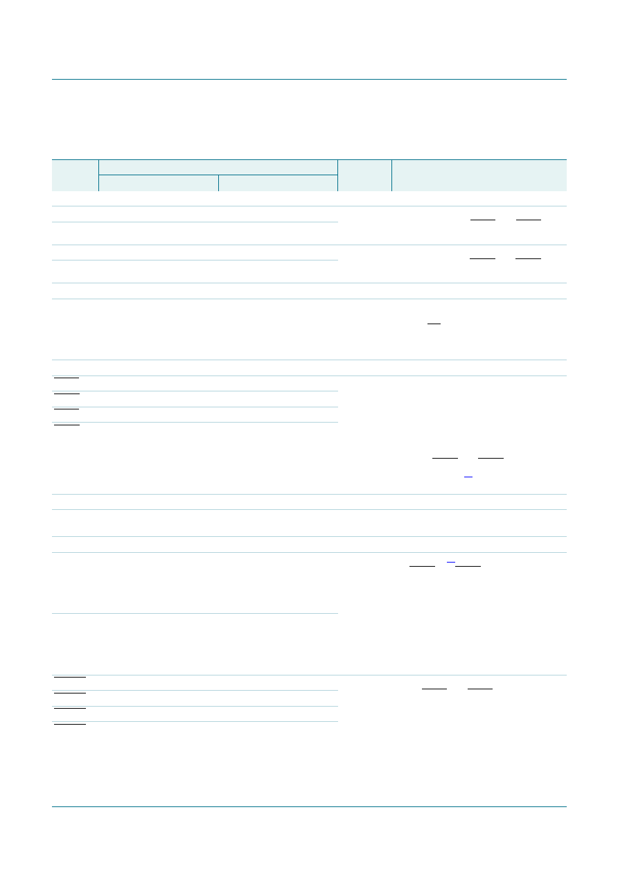
6.2 Pin description
Table 3.
Pin description
Symbol
Pin
Type
Description
1 : 2 Register A (C = 0)
1 : 2 Register B (C = 1)
Ungated inputs
DCKE0
D1
W1
SSTL_18
The outputs of this register will not be
suspended by the DCS0 and DCS1
control.
DCKE1
C1
Y1
DODT0
N1
K1
SSTL_18
The outputs of this register will not be
suspended by the DCS0 and DCS1
control.
DODT1
P1
J1
Chip Select gated inputs
D1 to
D28
A2, A1, B2, B1, C2, C1,
D2, D1, E1, F1, G1, H1,
N1, P1, R1, T1, U1, V1,
W1, W2, Y1, Y2, AA1,
AA2, AB1, AB2
A2, A1, B2, B1, C2, C1,
D2, D1, E1, F1, G1, H1, J1,
K1, N1, P1, R1, T1, U1,
V1, W1, W2, Y1, Y2, AA1,
AA2, AB1, AB2
SSTL_18
Data inputs, clocked in on the crossing of
the rising edge of CK and the falling
edge of CK.
Chip Select inputs
DCS0
K1
N1
SSTL_18
Chip select inputs. These pins initiate
DRAM address/command decodes, and
as such at least one will be LOW when a
valid address/command is present. The
register can be programmed to re-drive
all D-inputs (CSGEN = HIGH) only when
at least one chip select input is LOW. If
CSGEN, DCS0 and DCS1 inputs are
HIGH, D1 to D28[1] inputs will be
disabled.
DCS1
J1
P1
DCS2
K3
DCS3
P3
Conguration control inputs
C
A3
LVCMOS
input
Conguration control inputs; Register A
or Register B
Re-driven outputs
Q1A to
Q28A
A7, B7, C7, D7, E7, E2, F7,
F2, G7, G2, H7, H2, N2,
P2, R2, R7, T2, T7, U2,
U7, V2, V7, W7, Y7, AA7,
AB7
A7, B7, C7, D7, E7, E2, F7,
F2, G7, G2, H7, H2, J2,
K2, N2, P2, R2, R7, T2, T7,
U2, U7, V2, V7, W7, Y7,
AA7, AB7
1.8 V
CMOS
outputs
Data outputs[2] that are suspended by
the DCS0 and DCS1 control.
Q1B to
Q28B
A8, B8, C8, D8, E8, F8,
G8, H8, J8, J7, K8, K7, L8,
L7, M7, M8, N7, N8, P7,
P8, R8, T8, V8, U8, W8,
Y8, AA8, AB8
A8, B8, C8, D8, E8, F8,
G8, H8, J8, J7, K8, K7, L8,
L7, M7, M8, N7, N8, P7,
P8, R8, T8, U8, V8, W8,
Y8, AA8, AB8
QCS0A
K2
N2
1.8 V
CMOS
outputs
Data outputs that will not be suspended
by the DCS0 and DCS1 control.
QCS0B
L7
M7
QCS1A
J2
P2
QCS1B
L8
M8
相关PDF资料 |
PDF描述 |
|---|---|
| SSTUP32866EC/S | 32866 SERIES, POSITIVE EDGE TRIGGERED D FLIP-FLOP, COMPLEMENTARY OUTPUT, PBGA96 |
| SSTV16857EC | POSITIVE EDGE TRIGGERED D FLIP-FLOP, TRUE OUTPUT, PBGA56 |
| SSTV16859DGG,118 | SSTV SERIES, POSITIVE EDGE TRIGGERED D FLIP-FLOP, TRUE OUTPUT, PDSO64 |
| SSTV16859BS,118 | SSTV SERIES, POSITIVE EDGE TRIGGERED D FLIP-FLOP, TRUE OUTPUT, PQCC56 |
| SSTV16859EC,518 | SSTV SERIES, POSITIVE EDGE TRIGGERED D FLIP-FLOP, TRUE OUTPUT, PBGA96 |
相关代理商/技术参数 |
参数描述 |
|---|---|
| SSTUG32868ETS | 制造商:PHILIPS 制造商全称:NXP Semiconductors 功能描述:1.8 V 28-bit 1 : 2 configurable registered buffer with parity for DDR2-1G RDIMM applications |
| SSTUG32868G | 制造商:PHILIPS 制造商全称:NXP Semiconductors 功能描述:1.8 V 28-bit 1 : 2 configurable registered buffer with parity for DDR2-1G RDIMM applications |
| SSTUH32864 | 制造商:PHILIPS 制造商全称:NXP Semiconductors 功能描述:1.8 V high output drive configurable registered buffer for DDR2 RDIMM applications |
| SSTUH32864EC | 功能描述:寄存器 1.8V CONFIG REG BUFFER/DDRII RoHS:否 制造商:NXP Semiconductors 逻辑类型:CMOS 逻辑系列:HC 电路数量:1 最大时钟频率:36 MHz 传播延迟时间: 高电平输出电流:- 7.8 mA 低电平输出电流:7.8 mA 电源电压-最大:6 V 最大工作温度:+ 125 C 封装 / 箱体:SOT-38 封装:Tube |
| SSTUH32864EC,518 | 功能描述:寄存器 1.8V CONFIG REG RoHS:否 制造商:NXP Semiconductors 逻辑类型:CMOS 逻辑系列:HC 电路数量:1 最大时钟频率:36 MHz 传播延迟时间: 高电平输出电流:- 7.8 mA 低电平输出电流:7.8 mA 电源电压-最大:6 V 最大工作温度:+ 125 C 封装 / 箱体:SOT-38 封装:Tube |
发布紧急采购,3分钟左右您将得到回复。