- 您现在的位置:买卖IC网 > PDF目录98143 > SSTUG32868ET/G (NXP SEMICONDUCTORS) 32868 SERIES, POSITIVE EDGE TRIGGERED D FLIP-FLOP, COMPLEMENTARY OUTPUT, PBGA176 PDF资料下载
参数资料
| 型号: | SSTUG32868ET/G |
| 厂商: | NXP SEMICONDUCTORS |
| 元件分类: | 锁存器 |
| 英文描述: | 32868 SERIES, POSITIVE EDGE TRIGGERED D FLIP-FLOP, COMPLEMENTARY OUTPUT, PBGA176 |
| 封装: | 6 X 15 MM, 0.70 MM PITCH, LEAD FREE, PLASTIC, MO-246, SOT932-1, TFBGA-176 |
| 文件页数: | 29/29页 |
| 文件大小: | 166K |
| 代理商: | SSTUG32868ET/G |
第1页第2页第3页第4页第5页第6页第7页第8页第9页第10页第11页第12页第13页第14页第15页第16页第17页第18页第19页第20页第21页第22页第23页第24页第25页第26页第27页第28页当前第29页
SSTUG32868_1
NXP B.V. 2007. All rights reserved.
Product data sheet
Rev. 01 — 23 April 2007
9 of 29
NXP Semiconductors
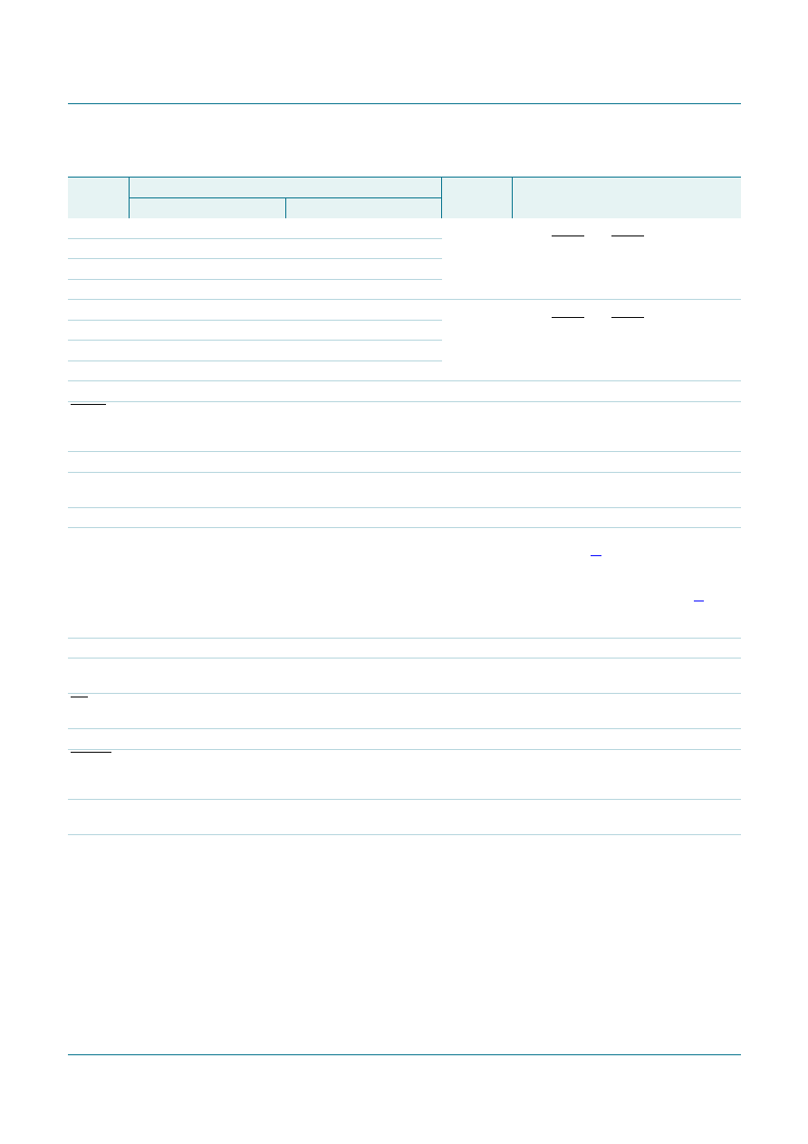
SSTUG32868
1.8 V DDR2-1G congurable registered buffer with parity
QCKE0A
F2
U2
1.8 V
CMOS
outputs
Data outputs that will not be suspended
by the DCS0 and DCS1 control.
QCKE0B
H8
R8
QCKE1A
E2
V2
QCKE1B
F8
U8
QODT0A N2
K2
1.8 V
CMOS
outputs
Data outputs that will not be suspended
by the DCS0 and DCS1 control.
QODT0B M7
L7
QODT1A P2
J2
QODT1B M8
L8
Output error
QERR
M3
open-drain
output
Output error bit; generated on clock
cycle after the corresponding data
output.
Parity input
PAR_IN
L3
SSTL_18
Parity input. Arrives one clock cycle after
the corresponding data input.
Program inputs
CSGEN
L2
LVCMOS
input
Chip select gate enable. When HIGH,
the D1 to D28[1] inputs will be latched
only when at least one chip select input
is LOW during the rising edge of the
clock. When LOW, the D1 to D28[1]
inputs will be latched and re-driven on
every rising edge of the clock.
Clock inputs
CK
L1
differential
input
Positive master clock input.
CK
M1
differential
input
Negative master clock input.
Miscellaneous inputs
RESET
M2
LVCMOS
input
Asynchronous reset input. Resets
registers and disables VREF data and
clock differential-input receivers.
VREF
A5, AB5
0.9 V
nominal
Input reference voltage.
VDD
B3, B4, B5, B6, D3, D4,
D5, D6, F3, F4, F5, F6, H3,
H4, H5, H6, K4, K5, K6,
M4, M5, M6, P4, P5, P6,
T3, T4, T5, T6, V3, V4, V5,
V6, Y3, Y4, Y5, Y6, AB4,
AB6
B3, B4, B5, B6, D3, D4,
D5, D6, F3, F4, F5, F6, H3,
H4, H5, H6, K4, K5, K6,
M4, M5, M6, P4, P5, P6,
T3, T4, T5, T6, V3, V4, V5,
V6, Y3, Y4, Y5, Y6, AB4,
AB6
1.8 V
nominal
Power supply voltage.
Table 3.
Pin description …continued
Symbol
Pin
Type
Description
1 : 2 Register A (C = 0)
1 : 2 Register B (C = 1)
相关PDF资料 |
PDF描述 |
|---|---|
| SSTUP32866EC/S | 32866 SERIES, POSITIVE EDGE TRIGGERED D FLIP-FLOP, COMPLEMENTARY OUTPUT, PBGA96 |
| SSTV16857EC | POSITIVE EDGE TRIGGERED D FLIP-FLOP, TRUE OUTPUT, PBGA56 |
| SSTV16859DGG,118 | SSTV SERIES, POSITIVE EDGE TRIGGERED D FLIP-FLOP, TRUE OUTPUT, PDSO64 |
| SSTV16859BS,118 | SSTV SERIES, POSITIVE EDGE TRIGGERED D FLIP-FLOP, TRUE OUTPUT, PQCC56 |
| SSTV16859EC,518 | SSTV SERIES, POSITIVE EDGE TRIGGERED D FLIP-FLOP, TRUE OUTPUT, PBGA96 |
相关代理商/技术参数 |
参数描述 |
|---|---|
| SSTUG32868ETS | 制造商:PHILIPS 制造商全称:NXP Semiconductors 功能描述:1.8 V 28-bit 1 : 2 configurable registered buffer with parity for DDR2-1G RDIMM applications |
| SSTUG32868G | 制造商:PHILIPS 制造商全称:NXP Semiconductors 功能描述:1.8 V 28-bit 1 : 2 configurable registered buffer with parity for DDR2-1G RDIMM applications |
| SSTUH32864 | 制造商:PHILIPS 制造商全称:NXP Semiconductors 功能描述:1.8 V high output drive configurable registered buffer for DDR2 RDIMM applications |
| SSTUH32864EC | 功能描述:寄存器 1.8V CONFIG REG BUFFER/DDRII RoHS:否 制造商:NXP Semiconductors 逻辑类型:CMOS 逻辑系列:HC 电路数量:1 最大时钟频率:36 MHz 传播延迟时间: 高电平输出电流:- 7.8 mA 低电平输出电流:7.8 mA 电源电压-最大:6 V 最大工作温度:+ 125 C 封装 / 箱体:SOT-38 封装:Tube |
| SSTUH32864EC,518 | 功能描述:寄存器 1.8V CONFIG REG RoHS:否 制造商:NXP Semiconductors 逻辑类型:CMOS 逻辑系列:HC 电路数量:1 最大时钟频率:36 MHz 传播延迟时间: 高电平输出电流:- 7.8 mA 低电平输出电流:7.8 mA 电源电压-最大:6 V 最大工作温度:+ 125 C 封装 / 箱体:SOT-38 封装:Tube |
发布紧急采购,3分钟左右您将得到回复。