- 您现在的位置:买卖IC网 > PDF目录69379 > ST7FMC2N6B6 (STMICROELECTRONICS) 8-BIT, FLASH, 8 MHz, MICROCONTROLLER, PDIP56 PDF资料下载
参数资料
| 型号: | ST7FMC2N6B6 |
| 厂商: | STMICROELECTRONICS |
| 元件分类: | 微控制器/微处理器 |
| 英文描述: | 8-BIT, FLASH, 8 MHz, MICROCONTROLLER, PDIP56 |
| 封装: | 0.600 INCH, PLASTIC, SDIP-56 |
| 文件页数: | 57/311页 |
| 文件大小: | 6511K |
| 代理商: | ST7FMC2N6B6 |
第1页第2页第3页第4页第5页第6页第7页第8页第9页第10页第11页第12页第13页第14页第15页第16页第17页第18页第19页第20页第21页第22页第23页第24页第25页第26页第27页第28页第29页第30页第31页第32页第33页第34页第35页第36页第37页第38页第39页第40页第41页第42页第43页第44页第45页第46页第47页第48页第49页第50页第51页第52页第53页第54页第55页第56页当前第57页第58页第59页第60页第61页第62页第63页第64页第65页第66页第67页第68页第69页第70页第71页第72页第73页第74页第75页第76页第77页第78页第79页第80页第81页第82页第83页第84页第85页第86页第87页第88页第89页第90页第91页第92页第93页第94页第95页第96页第97页第98页第99页第100页第101页第102页第103页第104页第105页第106页第107页第108页第109页第110页第111页第112页第113页第114页第115页第116页第117页第118页第119页第120页第121页第122页第123页第124页第125页第126页第127页第128页第129页第130页第131页第132页第133页第134页第135页第136页第137页第138页第139页第140页第141页第142页第143页第144页第145页第146页第147页第148页第149页第150页第151页第152页第153页第154页第155页第156页第157页第158页第159页第160页第161页第162页第163页第164页第165页第166页第167页第168页第169页第170页第171页第172页第173页第174页第175页第176页第177页第178页第179页第180页第181页第182页第183页第184页第185页第186页第187页第188页第189页第190页第191页第192页第193页第194页第195页第196页第197页第198页第199页第200页第201页第202页第203页第204页第205页第206页第207页第208页第209页第210页第211页第212页第213页第214页第215页第216页第217页第218页第219页第220页第221页第222页第223页第224页第225页第226页第227页第228页第229页第230页第231页第232页第233页第234页第235页第236页第237页第238页第239页第240页第241页第242页第243页第244页第245页第246页第247页第248页第249页第250页第251页第252页第253页第254页第255页第256页第257页第258页第259页第260页第261页第262页第263页第264页第265页第266页第267页第268页第269页第270页第271页第272页第273页第274页第275页第276页第277页第278页第279页第280页第281页第282页第283页第284页第285页第286页第287页第288页第289页第290页第291页第292页第293页第294页第295页第296页第297页第298页第299页第300页第301页第302页第303页第304页第305页第306页第307页第308页第309页第310页第311页
ST7MC1/ST7MC2
15/308
Notes:
1. In the interrupt input column, “eiX” defines the associated external interrupt vector. If the weak pull-up
column (wpu) is merged with the interrupt column (int), then the I/O configuration is pull-up interrupt input,
else the configuration is floating interrupt input.
2. If two alternate function outputs are enabled at the same time on a given pin (for instance, MCPWMV
and MCDEM on PD1 on LQFP32), the two signals will be ORed on the output pin.
3. MCES is a floating input. To disable this function, a pull-up resistor must be used.
4. OSC1 and OSC2 pins connect a crystal/ceramic resonator or an external source to the on-chip oscilla-
tor; see Section 1 INTRODUCTION and Section 12.5 CLOCK AND TIMING CHARACTERISTICS for
more details.
5. MCCFI can be mapped on 2 different pins on 80 ,64 and 56-pin packages. This allows:
- either to use PC1 as a standard I/O and map MCCFI on OAZ (MCCFI1) with or without using the oper-
ational amplifier (selected case after reset),
- or to map MCCFI on PC1 (MCCFI0) and use the amplifier for another function.
The mapping can be selected in MREF register of motor control cell. See section MOTOR CONTROL for
more details.
6. MCZEM is mapped on PF1 on 80, 64 and 56-pin packages and on PD2 on 44 and 32-pins.
MCDEM is mapped on PF0 on 80, 64 and 56-pin packages and on PD1 on 44 and 32-pin packages.
7. MCPWMV is mapped on PC6 on 80 and 64-pin packages and on PD1 on 44,and 32-pins packages.
MCPWMW is mapped on PC7 on 80, 64 and 44-pin packages and on PD0 on 32-pins package.
8. On the chip, each I/O port has 8 pads. Pads that are not bonded to external pins are in input pull-up
configuration after reset. The configuration of these pads must be kept at reset state to avoid added cur-
rent consumption. Refer to section 15.6 on page 302
9. Once the MTC peripheral is ON (bits CKE=1 or DAC=1 in the register MCRA), the pin PC4 is configured
to an alternate function. PC4 is no longer usable as a digital I/O.
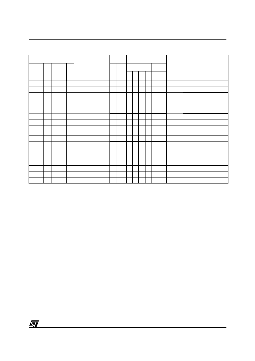
69
--
---
PH6
I/O TT
X XX
X
Port H6
70
--
---
PH7
I/O TT
X XX
X
Port H7
71 55
56
37
-
PE0/
OCMP2_B
I/O CT HS X XX
X
Port E0
Timer B Output Compare
2
72 56
1
38
-
PE1/
OCMP1_B
I/O CT
X XX
X
Port E1
Timer B Output Compare
1
73 57
2
39
-
PE2/ICAP2_B
I/O CT
X X
X
Port E2
Timer B Input Capture 2
74 58
3
40
-
PE3/ICAP1_B/ I/O CT
X X
X
Port E3
Timer B Input Capture 1
75 59
-
PE4/
EXTCLK_B
I/O CT
X XX
X
Port E4
Timer B External Clock
source
76 60
-
PE5
I/O CT
X XX
X
Port E5
77 614411
29
VPP/ICCSEL
I
Must be tied low. In the program-
ming mode when available, this pin
acts as the programming voltage in-
78 62
5
42
2
30
MCO0 (HS)
O
HS
X
MTC Output Channel 0
79 63
6
43
3
31
MCO1 (HS)
O
HS
X
MTC Output Channel 1
80 64
7
44
4
32
MCO2 (HS)
O
HS
X
MTC Output Channel 2
Table 1. ST7MC Device Pin Description
Pin n°
Pin Name
Type
Level
Port
Main
function
(after
reset)
Alternate function 2)
LQFP80
LQFP64
SDIP56
LQFP44
SDIP32
LQFP32
Input
Output
Input
Output
fl
oat
wp
u
int
ana
OD
PP
1
相关PDF资料 |
PDF描述 |
|---|---|
| ST7FMC2S6T6 | 8-BIT, FLASH, 8 MHz, MICROCONTROLLER, PQFP44 |
| ST7PMC2M9T6/XXX | 8-BIT, FLASH, 8 MHz, MICROCONTROLLER, PQFP80 |
| ST7PMC2R6T6/XXX | 8-BIT, FLASH, 8 MHz, MICROCONTROLLER, PQFP64 |
| ST7MC2N6B6 | MICROCONTROLLER, PDIP56 |
| ST7MC2M9T3 | MICROCONTROLLER, QFP80 |
相关代理商/技术参数 |
参数描述 |
|---|---|
| ST7FMC2N6T3 | 制造商:STMICROELECTRONICS 制造商全称:STMicroelectronics 功能描述:8-bit MCU with nested interrupts, Flash, 10-bit ADC, brushless motor control, five timers, SPI, LINSCI? |
| ST7FMC2N6T6 | 制造商:STMICROELECTRONICS 制造商全称:STMicroelectronics 功能描述:8-bit MCU with nested interrupts, Flash, 10-bit ADC, brushless motor control, five timers, SPI, LINSCI? |
| ST7FMC2N7B3 | 制造商:STMICROELECTRONICS 制造商全称:STMicroelectronics 功能描述:8-bit MCU with nested interrupts, Flash, 10-bit ADC, brushless motor control, five timers, SPI, LINSCI? |
| ST7FMC2N7B6 | 制造商:STMICROELECTRONICS 制造商全称:STMicroelectronics 功能描述:8-bit MCU with nested interrupts, Flash, 10-bit ADC, brushless motor control, five timers, SPI, LINSCI? |
| ST7FMC2N7T3 | 制造商:STMICROELECTRONICS 制造商全称:STMicroelectronics 功能描述:8-bit MCU with nested interrupts, Flash, 10-bit ADC, brushless motor control, five timers, SPI, LINSCI? |
发布紧急采购,3分钟左右您将得到回复。