- 您现在的位置:买卖IC网 > PDF目录69378 > ST7PLITEUS5U3TR (STMICROELECTRONICS) 8-BIT, FLASH, 8 MHz, MICROCONTROLLER, DSO8 PDF资料下载
参数资料
| 型号: | ST7PLITEUS5U3TR |
| 厂商: | STMICROELECTRONICS |
| 元件分类: | 微控制器/微处理器 |
| 英文描述: | 8-BIT, FLASH, 8 MHz, MICROCONTROLLER, DSO8 |
| 封装: | LEAD FREE, DFN-8 |
| 文件页数: | 104/108页 |
| 文件大小: | 1957K |
| 代理商: | ST7PLITEUS5U3TR |
第1页第2页第3页第4页第5页第6页第7页第8页第9页第10页第11页第12页第13页第14页第15页第16页第17页第18页第19页第20页第21页第22页第23页第24页第25页第26页第27页第28页第29页第30页第31页第32页第33页第34页第35页第36页第37页第38页第39页第40页第41页第42页第43页第44页第45页第46页第47页第48页第49页第50页第51页第52页第53页第54页第55页第56页第57页第58页第59页第60页第61页第62页第63页第64页第65页第66页第67页第68页第69页第70页第71页第72页第73页第74页第75页第76页第77页第78页第79页第80页第81页第82页第83页第84页第85页第86页第87页第88页第89页第90页第91页第92页第93页第94页第95页第96页第97页第98页第99页第100页第101页第102页第103页当前第104页第105页第106页第107页第108页
ST7LITEUSx
95/108
14 DEVICE CONFIGURATION AND ORDERING INFORMATION
Each device is available for production in user pro-
grammable versions (FLASH) as well as in factory
coded versions (FASTROM).
ST7PLITEUS2 and ST7PLITEUS5 devices are
Factory Advanced Service Technique ROM (FAS-
TROM) versions: they are factory-programmed
XFlash devices.
ST7FLITEUS2 and ST7FLITEUS5 XFlash devices
are shipped to customers with a default program
memory content (FFh).
The FASTROM factory coded parts contain the
code supplied by the customer. This implies that
FLASH devices have to be configured by the cus-
tomer using the Option Bytes while the FASTROM
devices are factory-configured.
14.1 OPTION BYTES
The two option bytes allow the hardware configu-
ration of the microcontroller to be selected.
The option bytes can be accessed only in pro-
gramming mode (for example using a standard
ST7 programming tool).
OPTION BYTE 1
Bit 7:6 = CKSEL[1:0] Start-up clock selection.
This bit is used to select the startup frequency. By
default, the Internal RC is selected.
Bit 5 = Reserved, must always be 1.
Bit 4 = Reserved, must always be 0.
Bits 3:2 = LVD[1:0] Low Voltage Detection selec-
tion
These option bits enable the LVD block with a se-
lected threshold as shown in Table 23.
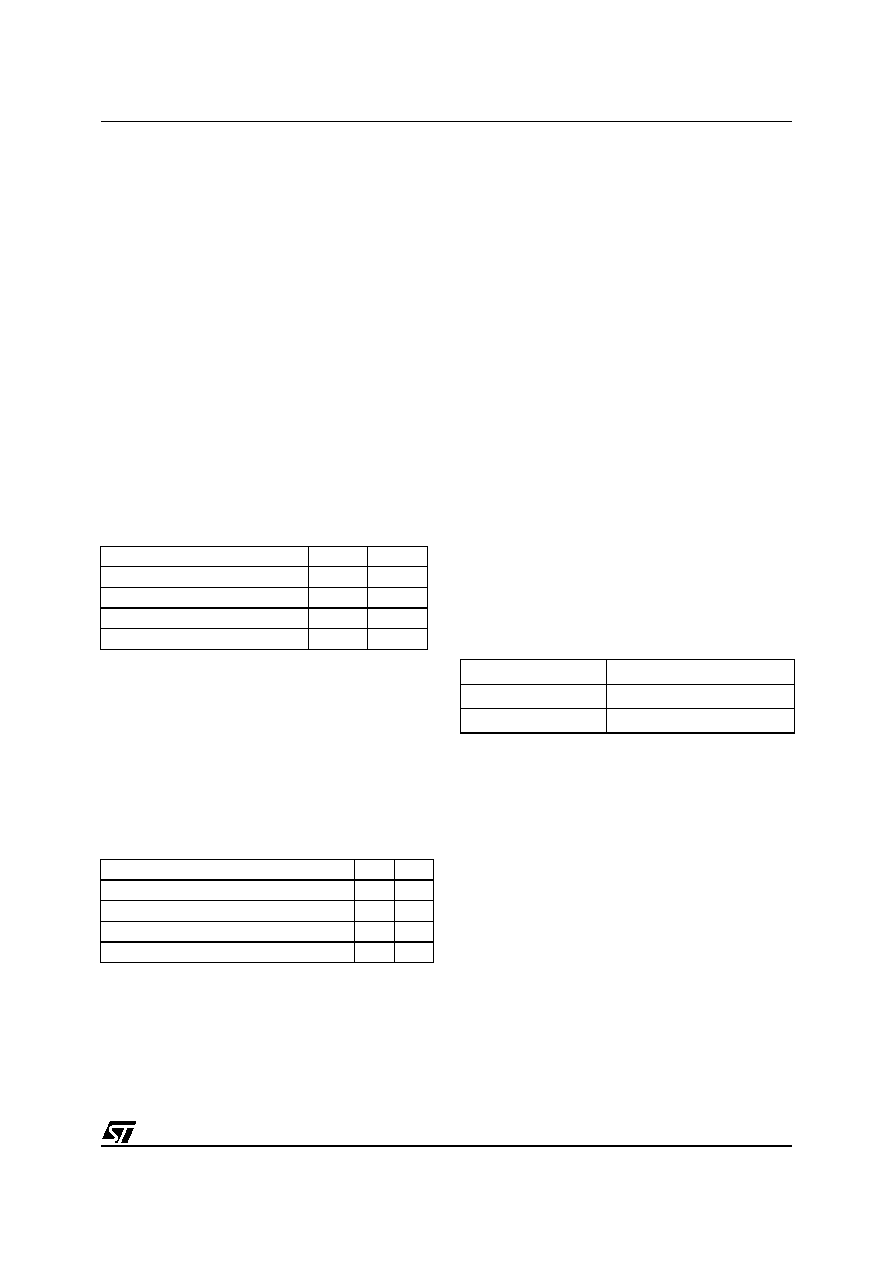
Table 23. LVD Threshold Configuration
Bit 1 = WDG SW Hardware or software watchdog
This option bit selects the watchdog type.
0: Hardware (watchdog always enabled)
1: Software (watchdog to be enabled by software)
Bit 0 = WDG HALT Watchdog Reset on Halt
This option bit determines if a RESET is generated
when entering HALT mode while the Watchdog is
active.
0: No Reset generation when entering Halt mode
1: Reset generation when entering Halt mode
OPTION BYTE 0
Bits 7:4 = Reserved, must always be 1.
Bit 3 = Reserved, must always be 0.
Bit 2 = SEC0 Sector 0 size definition
This option bit indicates the size of sector 0 ac-
cording to the following table.
Bit 1 = FMP_R Read-out protection
Readout protection, when selected provides a pro-
tection against program memory content extrac-
tion and against write access to Flash memory.
Erasing the option bytes when the FMP_R option
is selected will cause the whole memory to be
erased first, and the device can be reprogrammed.
Refer to Section 4.5 and the ST7 Flash Program-
ming Reference Manual for more details.
0: Read-out protection off
1: Read-out protection on
Bit 0 = FMP_W FLASH write protection
This option indicates if the FLASH program mem-
ory is write protected.
Warning: When this option is selected, the pro-
gram memory (and the option bit itself) can never
be erased or programmed again.
0: Write protection off
1: Write protection on
Configuration
CKSEL1 CKSEL0
Internal RC as Startup Clock
0
AWU RC as a Startup Clock
0
1
Reserved
1
0
External Clock on pin PA5
1
Configuration
LVD1 LVD0
LVD Off
1
Highest Voltage Threshold
1
0
Medium Voltage Threshold
0
1
Lowest Voltage Threshold
0
Sector 0 Size
SEC0
0.5k
0
1k
1
相关PDF资料 |
PDF描述 |
|---|---|
| ST7PLITEUS5M6TR | 8-BIT, MROM, 8 MHz, MICROCONTROLLER, PDSO8 |
| ST7PLITEUS5M6 | 8-BIT, MROM, 8 MHz, MICROCONTROLLER, PDSO8 |
| ST7FLITEUS5M3TR | 8-BIT, FLASH, 8 MHz, MICROCONTROLLER, PDSO8 |
| ST7FLITEUS2B3 | 8-BIT, FLASH, 8 MHz, MICROCONTROLLER, PDIP8 |
| ST7FSCR1E4U1 | 8-BIT, FLASH, 8 MHz, MICROCONTROLLER, QCC64 |
相关代理商/技术参数 |
参数描述 |
|---|---|
| ST7PLITEUS5U6 | 制造商:STMICROELECTRONICS 制造商全称:STMicroelectronics 功能描述:8-bit MCU with single voltage Flash memory, ADC, timers |
| ST7PLITEUS5U6TR | 制造商:STMICROELECTRONICS 制造商全称:STMicroelectronics 功能描述:8-bit MCU with single voltage Flash memory, ADC, timers |
| ST7PMC1K2B3 | 制造商:STMICROELECTRONICS 制造商全称:STMicroelectronics 功能描述:8-bit MCU with nested interrupts, Flash, 10-bit ADC, brushless motor control, five timers, SPI, LINSCI? |
| ST7PMC1K2B6 | 制造商:STMICROELECTRONICS 制造商全称:STMicroelectronics 功能描述:8-BIT MCU WITH NESTED INTERRUPTS, FLASH, 10-BIT ADC, BRUSHLESS MOTOR CONTROL, FIVE TIMERS, SPI, LINSCI |
| ST7PMC1K2T3 | 制造商:STMICROELECTRONICS 制造商全称:STMicroelectronics 功能描述:8-bit MCU with nested interrupts, Flash, 10-bit ADC, brushless motor control, five timers, SPI, LINSCI? |
发布紧急采购,3分钟左右您将得到回复。